Method for checking, evaluation, and/or error diagnosis of a sensor system, sensor system, and system
- Summary
- Abstract
- Description
- Claims
- Application Information
AI Technical Summary
Benefits of technology
Problems solved by technology
Method used
Image
Examples
Embodiment Construction
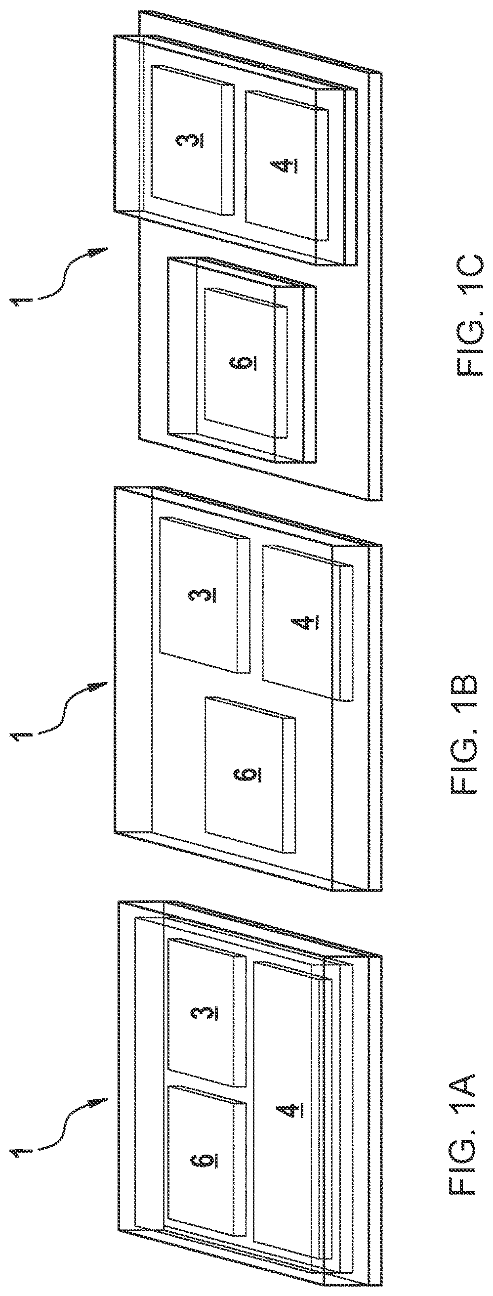
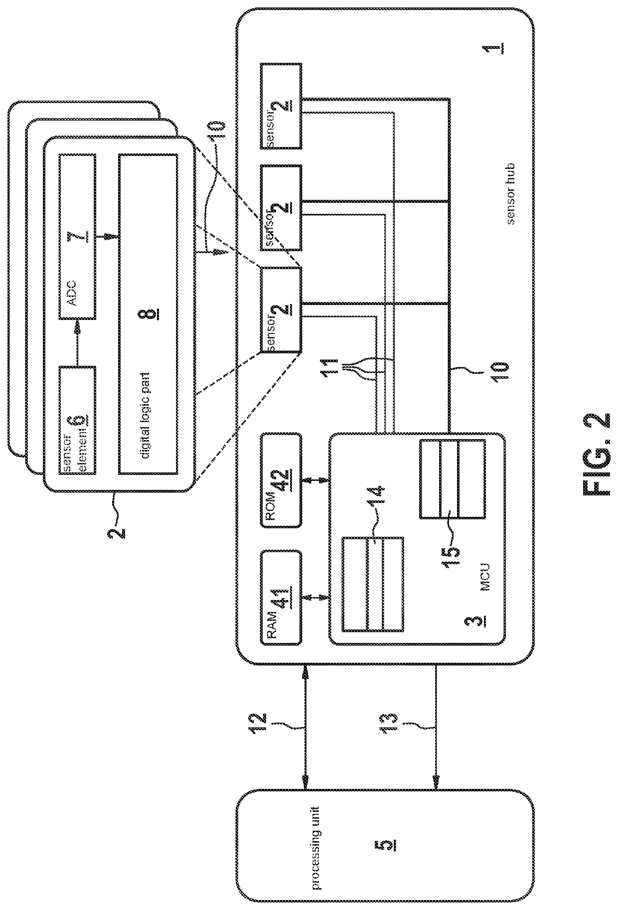
[0034]Intelligent sensors may be classified into three different integration levels, which are shown in FIGS. 1A-1C. The version having the highest integration is the SoC (system-on-chip), shown in FIG. 1A. All components 3, 4, 6 are placed on the same die of a semiconductor wafer. In the case of an intelligent sensor, there are at least one MEMS element 6, an application processor 3, and a memory element 4 (primarily RAM). The second integration level in FIG. 1B shows a system-in-package (SiP). Some components are placed in the same housing and are connected to one another via lines. MEMS element 6, microcontroller 3, and flash memory 4 are located on dedicated dies, but in the same housing. The lowest integration level is offered by the system-on-module (SoM) implementation of a smart sensor shown in FIG. 1C. Each system component 3, 4, 6 has its own housing and all components 3, 4, 6 are placed on the same circuit board. The sensor-in-the-loop concept according to the present inv...
PUM
 Abstract
Description
Claims
Application Information


