
Dram having deep trench capacitors with lightly doped buried plates

Inactive Publication Date: 2009-07-09
GLOBALFOUNDRIES INC
View PDF14 Cites 39 Cited by
  • Summary
  • Abstract
  • Description
  • Claims
  • Application Information

AI Technical Summary

Benefits of technology

[0117]The “one-size-fits-all era” of eDRAM is over. For different applications, different DRAM designs are needed to optimize performance, power consumption or packing density. There clearly are many cases where these different design needs need to be integrated on the same chip. For example, (i) a conventional eDRAM with 128 ms retention which requires larger DT capacitance than that required by a high performance eDRAM macro that is developed on the same test site. The current process is we either get the optimized capacitance for the conventional macro or the optimized capacitance for the high performance macro—we cannot get both without significantly complicating the process. Another example is the increasing bits and areas of L2 and L3 cache calling for the on-chip integration of eDRAM to replace bulky SRAM which is also suffering from escalated soft error rate (SER). As high performance eDRAM macros are developed, a need will arise to use high performance eDRAM as L2 cache and conventional / more dense eDRAMs as L3 cache. In short, the ability to create different DT capacitors on the same chip at low cost can significantly reduce development cost and in the future offer attractive alternatives to SRAM cache on microprocessors.
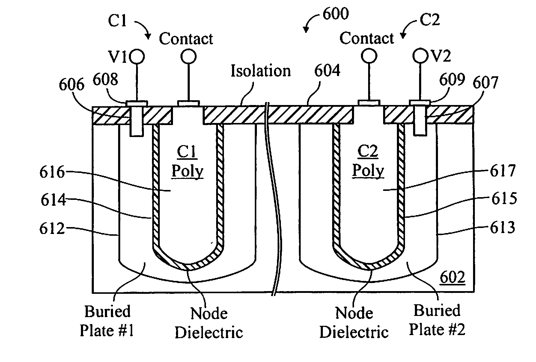
[0119]According to the invention, generally, by carefully controlling plate doping level and plate bias condition, different DT capacitances can be obtained on the same chip with the same layout and DT process. Two immediate advantages are (1) two designs with different DT capacitance requirement can be merged on the same test site and run an identical DT process; (2) a high performance high retention eDRAM macro can be integrated on the same chip as level 2 and level 3 caches, respectively.

Problems solved by technology

This requires additional masks and at least two additional DT etch steps, which is a significant cost adder.

Method used


Image

  • Dram having deep trench capacitors with lightly doped buried plates
  • Dram having deep trench capacitors with lightly doped buried plates
  • Dram having deep trench capacitors with lightly doped buried plates

Examples


Embodiment Construction

[0140]In the description that follows, numerous details are set forth in order to provide a thorough understanding of the present invention. It will be appreciated by those skilled in the art that variations of these specific details are possible while still achieving the results of the present invention. Well-known processing steps and materials are generally not described in detail in order to avoid unnecessarily obfuscating the description of the present invention.

[0141]Throughout the descriptions set forth in this disclosure, lowercase numbers or letters may be used, instead of subscripts. For example Vg could be written Vg. Generally, lowercase is preferred to maintain uniform font size.) Regarding the use of subscripts (in the drawings, as well as throughout the text of this document), sometimes a character (letter or numeral) is written as a subscript—smaller, and lower than the character (typically a letter) preceding it, such as “Vs” (source voltage) or “H2O” (water). For c...


PUM


Abstract

By controlling buried plate doping level and bias condition, different capacitances can be obtained from capacitors on the same chip with the same layout and deep trench process. The capacitors may be storage capacitors of DRAM / eDRAM cells. The doping concentration may be less than 3E19cm−3, a voltage difference between the biases of the buried electrodes may be at least 0.5V, and a capacitance of one capacitor may be at least 1.2 times, such as 2.0 times the capacitance of another capacitor.

Description

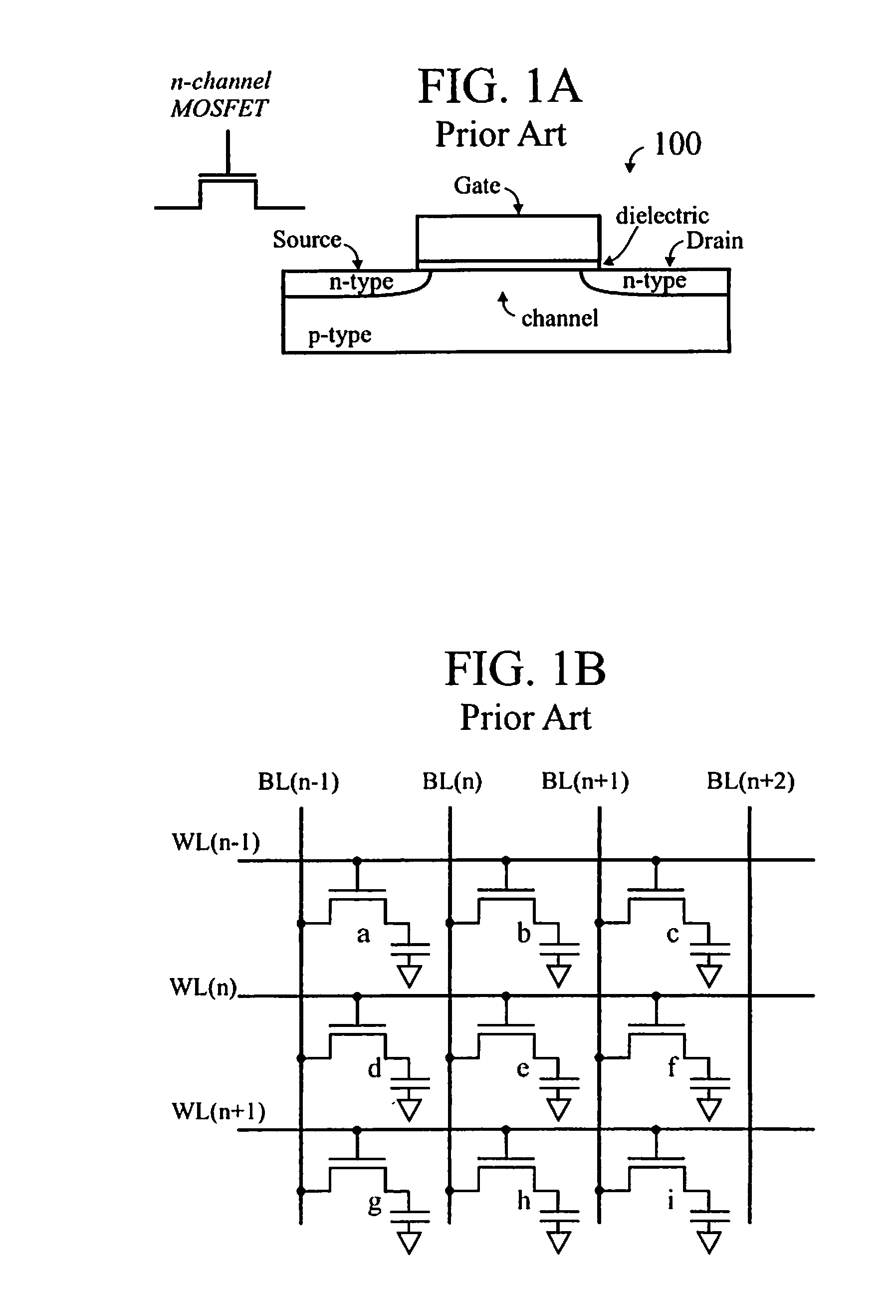
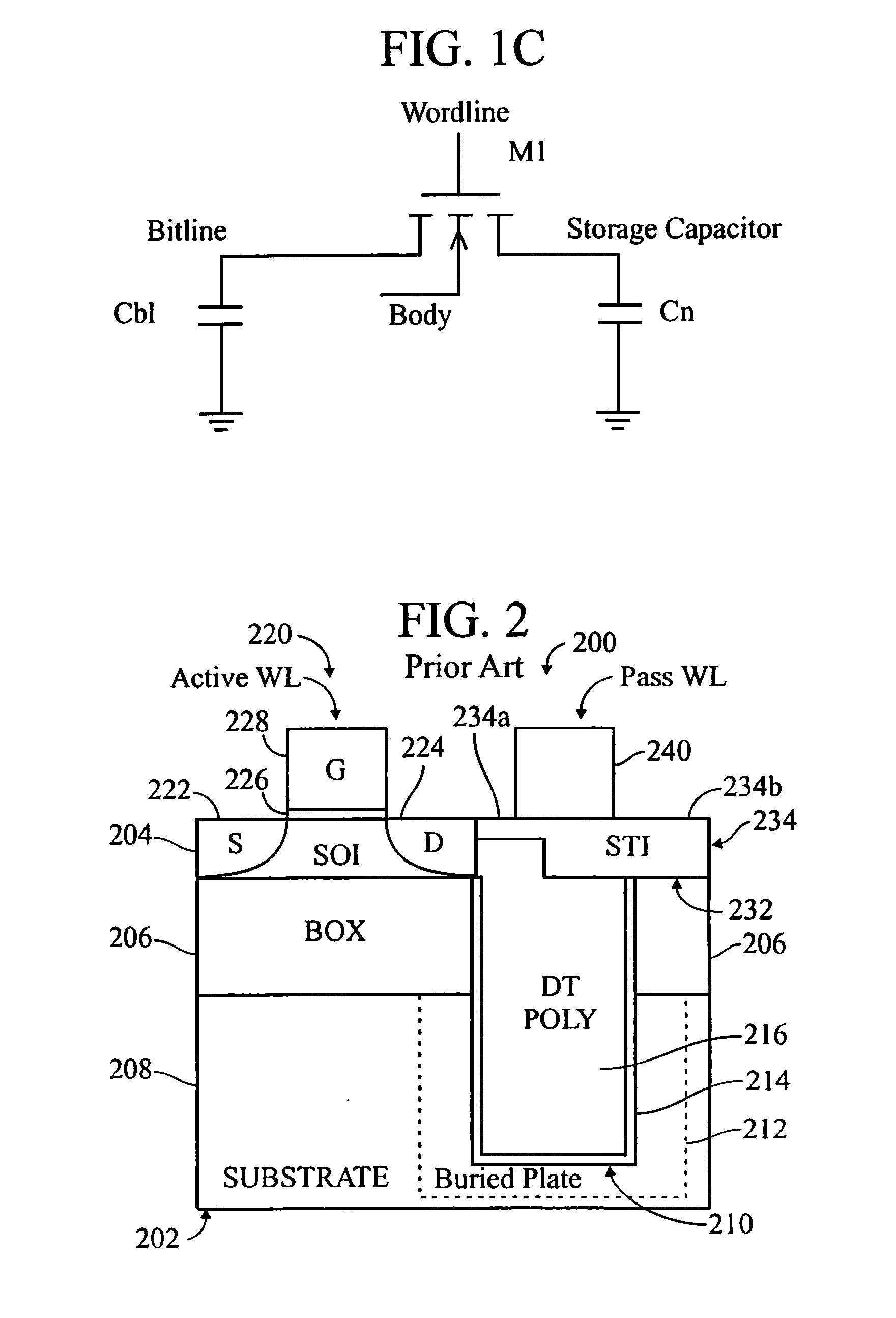
FIELD OF THE INVENTION[0001]The invention relates to dynamic random access memory (DRAM) and, more particularly to embedded DRAM (eDRAM) and, more particularly to deep trench (DT) capacitors used in DRAM.BACKGROUND OF THE INVENTION[0002]The transistor is a solid state semiconductor device which can be used for amplification, switching, voltage stabilization, signal modulation and many other functions. Generally, a transistor has three terminals, and a voltage applied to a specific one of the terminals controls current flowing between the other two terminals. One type of transistor is known as the field effect transistor (FET).[0003]The terminals of a field effect transistor (FET) are commonly named source, gate and drain. In the The transistor is a solid state semiconductor device which can be used for amplification, switching, voltage stabilization, signal modulation and many other functions. Generally, a transistor has three terminals, and a voltage applied to a specific one of th...

Claims


Application Information

Patent Timeline
IPC IPC(8): H01L29/92H01L21/28G06F17/50
CPCG11C11/404H01L29/66181H01L27/10861H01L27/0805H10B12/038
Inventor WANG, GENGCHENG, KANGGUOFALTERMEIER, JOHNATHAN E.PARRIES, PAUL C.
Owner GLOBALFOUNDRIES INC
Learn More