Method for forming semiconductor structure

a technology of semiconductor structure and filling material, which is applied in the direction of semiconductor/solid-state device manufacturing, basic electric elements, electric devices, etc., can solve the problems of affecting the performance of a beol circuit, affecting the normal operation of a semiconductor device, etc., and achieves the effect of reducing the requirement of filling material and simplifying the steps of forming

Pending Publication Date: 2022-03-31
SEMICON MFG INT (SHANGHAI) CORP +1
View PDF3 Cites 0 Cited by
  • Summary
  • Abstract
  • Description
  • Claims
  • Application Information

AI Technical Summary

Benefits of technology

[0006]To address the foregoing problem, forms of the present disclosure provide a method for forming a semiconductor structure, to improve the formation quality of a smaller-dimension interconnect structure in a BEOL process.
[0011]Compared to the related art, the technical solutions of the embodiments of the present disclosure have the following advantages.
[0014]Accordingly, a problem can be avoided that the photoresist peels off during etching due to an elongated shape when the mandrel lines separated on the base are formed through etching by directly using the photoresist as a mask in a process of forming a small-dimension pattern. Further, the first trench and the second trench are formed successively using two photolithography processes using different masks, and the subsequently formed separated mandrel lines are formed using the same material, which can simplify steps of forming the mandrel lines for the first time using the first etching process and then performing material filling and performing the second photolithography process when the mandrel lines are formed directly using a plurality of photolithography processes, and lower a requirement on the filled material.

Problems solved by technology

The formation quality of an interconnect structure significantly affects the performance of a BEOL circuit, or even affects normal operation of a semiconductor device.
Therefore, how to improve a formation quality of a smaller-dimension interconnect structure in the BEOL process has become a technical problem to be resolved urgently by a person skilled in the art.

Method used


Image

  • Method for forming semiconductor structure
  • Method for forming semiconductor structure
  • Method for forming semiconductor structure

Examples


Embodiment Construction

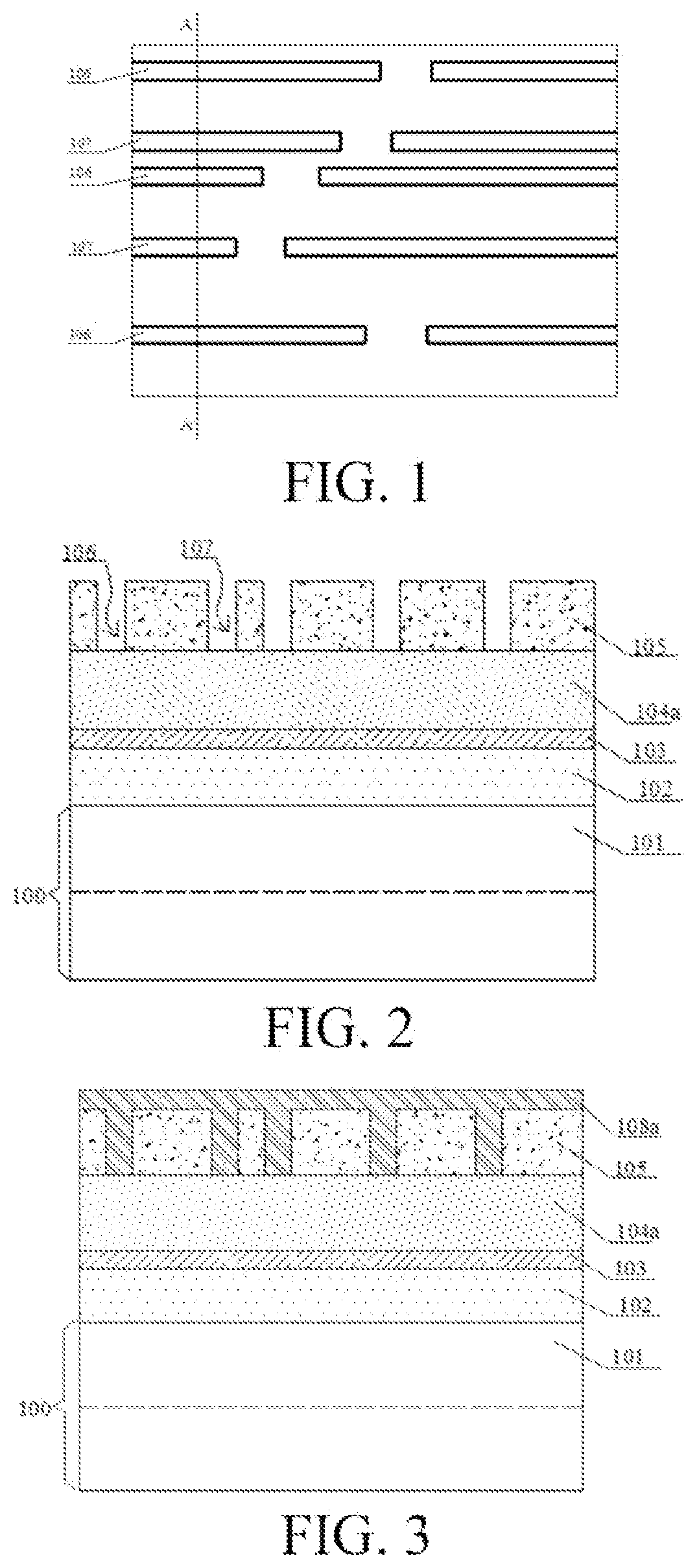
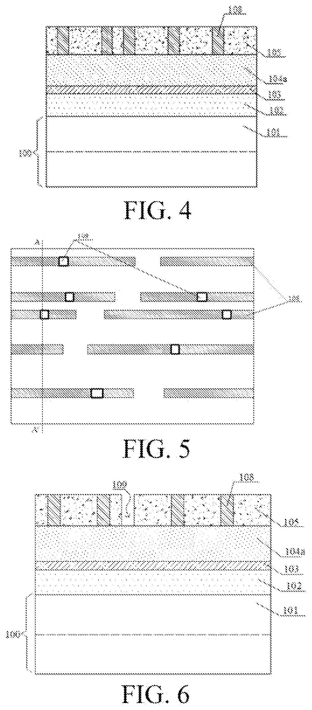
[0016]It can be seen from the related art that with the miniaturization and higher integration of components, a quantity of conductor connection lines in a circuit continuously increases.

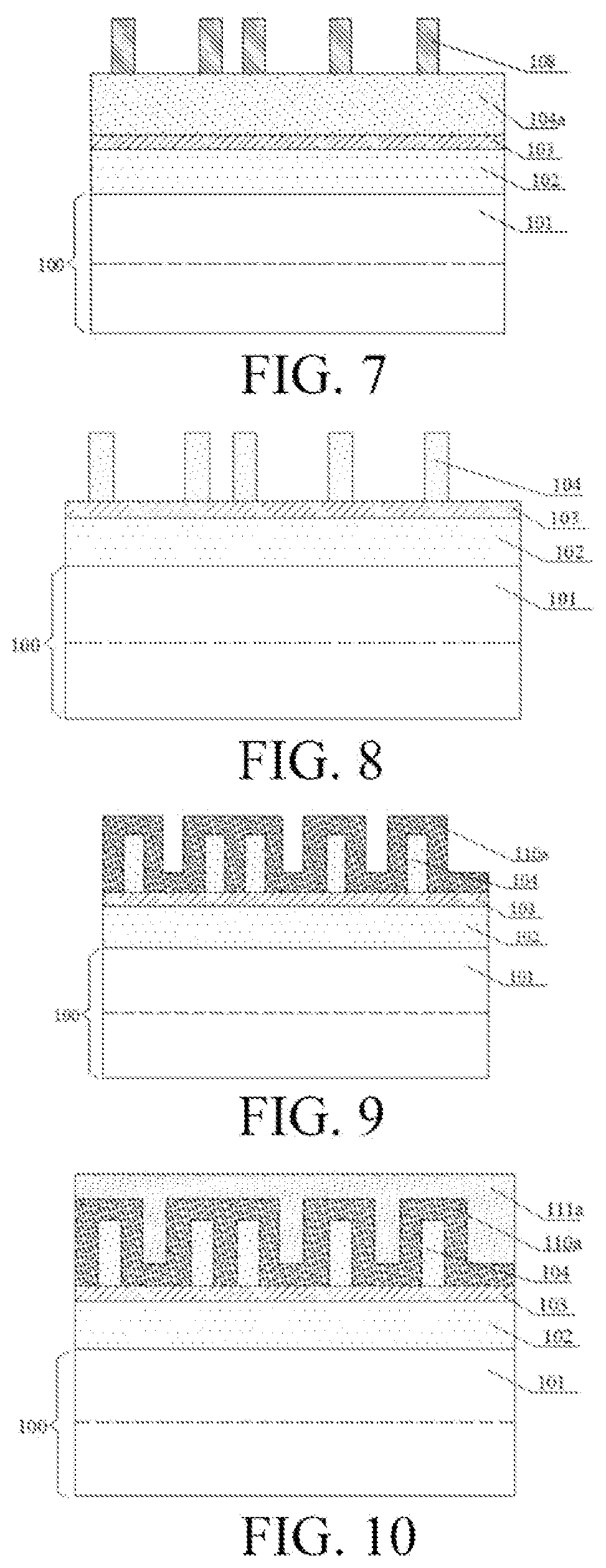
[0017]Because of the increasing quantity of conductor connection lines in the circuit, a pattern dimension of a metal interconnect line needs to be smaller, and a width of a pattern line of the IC needs to be smaller, leading to a higher requirement on a photolithography process. When an existing photolithography technology cannot meet a corresponding process requirement, a series of problems are likely to occur. For example, when at least two illuminations need to be performed to form a mandrel line, in a usual method, a first mandrel line is first formed through one photolithography process, and then material filling is performed around the first mandrel line to form a plane for a next illumination. An etch selectivity of a material filled around the first mandrel line to a material forming the fi...


PUM

PropertyMeasurementUnit
semiconductor structureaaaaaaaaaa
semiconductoraaaaaaaaaa
dimensionaaaaaaaaaa

Abstract

A method for forming a semiconductor structure is provided. In one form, a method includes: providing a base; forming a pattern memory layer on the base, where at least a first trench and a second trench are provided on the pattern memory layer, where an extending direction of the first trench is parallel to an extending direction of the second trench, and the first trench and the second trench are formed using different masks; and forming mandrel lines separated on the base at positions of the base that correspond to the first trench and the second trench. By using the method, a problem that a photoresist peels off during etching due to an elongated shape when separated mandrel lines are directly formed can be avoided. Further, a problem of a relatively high requirement on a filling material when the mandrel lines are formed directly by using a plurality of photolithography processes can be avoided, to lower the requirement on the filling material.

Description

RELATED APPLICATIONS[0001]The present application claims priority to Chinese Patent Appln. No. 202011061150.5, filed Sep. 30, 2020, the entire disclosure of which is hereby incorporated by reference.BACKGROUNDTechnical Field[0002]Embodiments of the present disclosure relate to the field of semiconductor manufacturing, and in particular, to a method for forming a semiconductor structure.Related Art[0003]As semiconductor manufacturing technologies become increasingly sophisticated, integrated circuits (ICs) are undergoing significant changes. A quantity of components integrated on the same chip has increased from an initial tens or hundreds components to millions of components. To meet the requirement on circuit density, a batch processing technology is used in a manufacturing process of a semiconductor IC chip to form different types of complex devices on a substrate, and interconnect the devices using an interconnect structure, to implement a complete electronic function of the chip...

Claims


Application Information

Patent Timeline
Patent Type & Authority Applications(United States)
IPC IPC(8): H01L21/768H01L21/033
CPCH01L21/76832H01L21/7684H01L21/76877H01L21/0338H01L21/76816H01L21/31144H01L21/0337
Inventor ZUOPENG, HEMING, YANGDUOHUI, BEI
Owner SEMICON MFG INT (SHANGHAI) CORP
Why Eureka
Try Eureka