Light-Emitting Device, Light-Emitting Appliance, Display Device, Electronic Appliance, and Lighting Device

a technology of light-emitting devices and light-emitting materials, which is applied in the direction of organic semiconductor devices, identification means, instruments, etc., can solve the problems of difficult design of light-emitting materials that simultaneously meet these two requirements, and the light-emitting devices that emit blue phosphorescence in particular have not yet been put into practical use, so as to achieve high emission efficiency and reduce power consumption. , the effect of high reliability of light-emitting devices

Pending Publication Date: 2022-05-05
SEMICON ENERGY LAB CO LTD
View PDF0 Cites 2 Cited by
  • Summary
  • Abstract
  • Description
  • Claims
  • Application Information

AI Technical Summary

Benefits of technology

[0038]According to one embodiment of the present invention, a light-emitting device with high emission efficiency can be provided. According to another embodiment of the present invention, a highly reliable light-emitting device can be provided. According to another embodiment of the present invention, a light-emitting device with reduced power consumption can be provided. According to another embodiment of the present invention, a novel light-emitting device can be provided. According to another embodiment of the present invention, a no

Problems solved by technology

Among light-emitting devices using phosphorescent materials, a light-emitting device that emits blue phosphorescence in particular has not yet been put into practical use because it is

Method used


Image

  • Light-Emitting Device, Light-Emitting Appliance, Display Device, Electronic Appliance, and Lighting Device
  • Light-Emitting Device, Light-Emitting Appliance, Display Device, Electronic Appliance, and Lighting Device
  • Light-Emitting Device, Light-Emitting Appliance, Display Device, Electronic Appliance, and Lighting Device

Examples


embodiment 1

[0069]In this embodiment, a light-emitting device of one embodiment of the present invention will be described below with reference to FIG. 1 to FIG. 5.

Structure Example of Light-Emitting Device

[0070]First, a structure of a light-emitting device of one embodiment of the present invention will be described below with reference to FIG. 1.

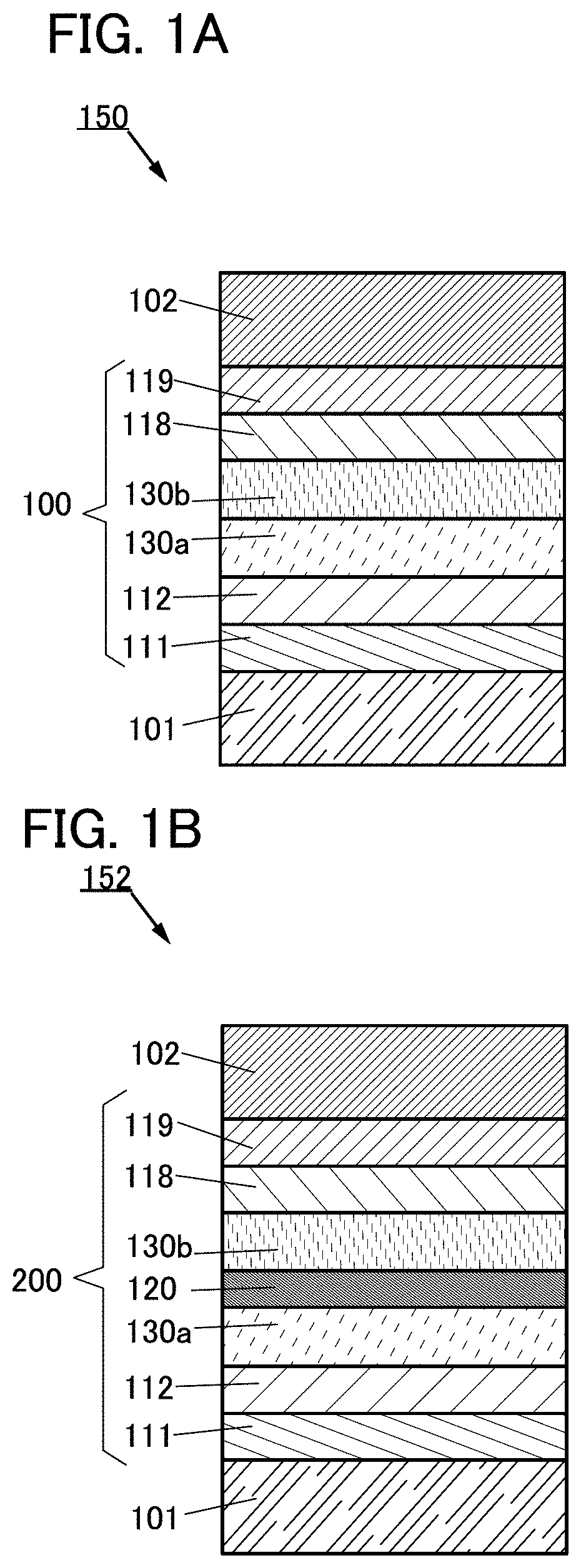
[0071]FIG. 1A and FIG. 1B are schematic cross-sectional views of a light-emitting device 150 and a light-emitting device 152 of one embodiment of the present invention.

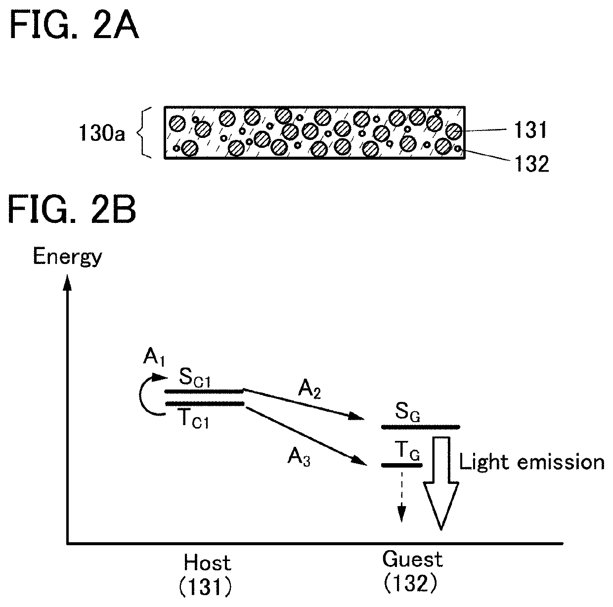
[0072]The light-emitting device 150 and the light-emitting device 152 each include a pair of electrodes (an electrode 101 and an electrode 102) and an EL layer 100 or an EL layer 200 provided between the pair of electrodes. The EL layer 100 and the EL layer 200 each include at least a light-emitting layer 130a and a light-emitting layer 130b.

[0073]The EL layer 100 illustrated in FIG. 1A includes, in addition to the light-emitting layer 130a and the light-emitting layer 130b, functional...

embodiment 2

[0382]In this embodiment, examples of a method for synthesizing an organic compound that is favorably used for the light-emitting device of one embodiment of the present invention will be described giving the organic compounds represented by General Formulae (G1) and (G2) as an example.

Method for Synthesizing Organic Compound Represented by General Formula (G1)

[0383]The organic compound represented by General Formula (G1) shown above can be synthesized by a synthesis method using a variety of reactions. For example, the organic compound can be synthesized by Synthesis Schemes (S-1) and (S-2) shown below. A compound 1, an arylamine (a compound 2), and an arylamine (a compound 3) are coupled, whereby a diamine compound (a compound 4) is obtained.

[0384]Next, the diamine compound (the compound 4), halogenated aryl (the compound 5), and halogenated aryl (the compound 6) are coupled, whereby the organic compound represented by General Formula (G1) can be obtained.

[0385]In Synthesis Scheme...

embodiment 3

[0409]In this embodiment, a light-emitting device having a structure different from the structure of the light-emitting device described in Embodiment 1 will be described below with reference to FIG. 12. Note that in FIG. 12, a portion having a function similar to that in FIG. 1A is represented by the same hatch pattern and a reference numeral thereof is omitted in some cases. In addition, common reference numerals are used for portions having similar functions, and a detailed description thereof is omitted in some cases.

Structure Example 2 of Light-Emitting Device

[0410]FIG. 12 is a schematic cross-sectional view of a light-emitting device 250.

[0411]The light-emitting device 250 illustrated in FIG. 12 includes a plurality of light-emitting units (a light-emitting unit 106 and a light-emitting unit 108) between a pair of electrodes (the electrode 101 and the electrode 102). Any one of the plurality of light-emitting units preferably has a structure similar to that of the EL layer 100...


PUM


Abstract

A light-emitting device with high emission efficiency and reliability is provided. The light-emitting device includes a fluorescent light-emitting layer and a phosphorescent light-emitting layer. A host material used in the fluorescent light-emitting layer has a function of converting triplet excitation energy into light emission and a guest material used in the fluorescent light-emitting layer emits fluorescence. The guest material has a molecular structure including a luminophore and a protecting group, and one molecule of the guest material includes five or more protecting groups. The introduction of the protecting groups into the molecule inhibits transfer of triplet excitation energy from the host material to the guest material by the Dexter mechanism. An alkyl group or a branched-chain alkyl group is used as the protecting group. The longest wavelength absorption band in the absorption spectrum of the guest material in the phosphorescent light-emitting layer has an overlap with the emission spectrum of the host material in the phosphorescent light-emitting layer.

Description

TECHNICAL FIELD[0001]One embodiment of the present invention relates to a light-emitting device, or a display device, an electronic appliance, and a lighting device including the light-emitting device.[0002]Note that one embodiment of the present invention is not limited to the above technical field. The technical field of one embodiment of the invention disclosed in this specification and the like relates to an object, a method, or a manufacturing method. Another embodiment of the present invention relates to a process, a machine, manufacture, or a composition of matter. Accordingly, specific examples of the technical field of one embodiment of the present invention disclosed in this specification include a semiconductor device, a display device, a liquid crystal display device, a light-emitting device, a lighting device, a power storage device, a memory device, a driving method thereof, and a manufacturing method thereof.BACKGROUND ART[0003]In recent years, research and developmen...

Claims


Application Information

Patent Timeline
IPC IPC(8): H01L51/50G06F3/041
CPCH01L51/5028H01L2251/552H01L2251/5384G06F3/041H05B33/12G09F9/30H10K85/633H10K50/121H10K50/13H10K2101/90Y02P20/55G09F9/335G09F9/301H10K85/00H10K85/631H10K85/346H10K85/654H10K85/6574H10K85/40H10K85/342H10K85/6572H10K2101/30
Inventor ISHISONE, TAKAHIROOHSAWA, NOBUHARUSEO, SATOSHI
Owner SEMICON ENERGY LAB CO LTD
Why Eureka
Try Eureka