
Method for coating chips

a technology of coating chips and coating films, applied in the field of coating chips, can solve the problems of limiting the size of the inter-chip space of the order of 500 m, the method known from the prior art is however not satisfactory, and the difference between the thermal expansion coefficient of the support substrate and the thermal expansion coefficient of the coating film can genera

Pending Publication Date: 2022-05-12
COMMISSARIAT A LENERGIE ATOMIQUE ET AUX ENERGIES ALTERNATIVES
View PDF0 Cites 0 Cited by
  • Summary
  • Abstract
  • Description
  • Claims
  • Application Information

AI Technical Summary

Benefits of technology

The present invention provides a method for coating semiconductor chips without applying a mechanical force to the chips. This method maintains the mechanical integrity of chips and can be used with chips having low mechanical strength on their surface elements. The coating film can be formed only at the inter-chip spaces, allowing for additional manufacturing steps on a relatively flat surface. The method also allows filling the entire inter-chip space by limiting or eliminating the formation of voids at the inter-chip spaces. The temperatures involved in this method allow maintaining the integrity of temperature-sensitive materials and limiting the relative expansion since the chip and the substrate are each made of materials having a different coefficient of thermal expansion. The photosensitive coating film has a positive tone.

Problems solved by technology

This method known from the prior art is however not satisfactory.
Moreover, a difference between the coefficients of thermal expansion of the support substrate and the coating film can generate, under the effect of this heating, constraints, and more particularly a detachment of the chips.
However, due to the presence of these beads of known average diameter, this solution limits the reduction in size of the inter-chip space of the order of 500 μm (5 times the conventional average diameter of the beads).
Furthermore, the third step, as proposed in the method known from the prior art, does not allow keeping said coating film exclusively at the inter-chip spaces and, recessed relative to the front faces of the chips, without degrading said front faces.

Method used


Image

  • Method for coating chips
  • Method for coating chips
  • Method for coating chips

Examples


Embodiment Construction

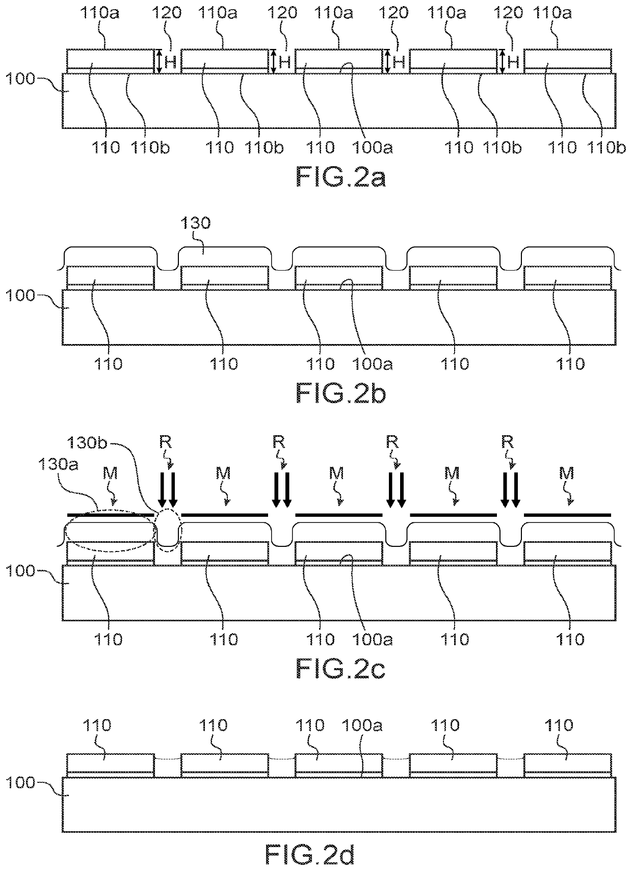
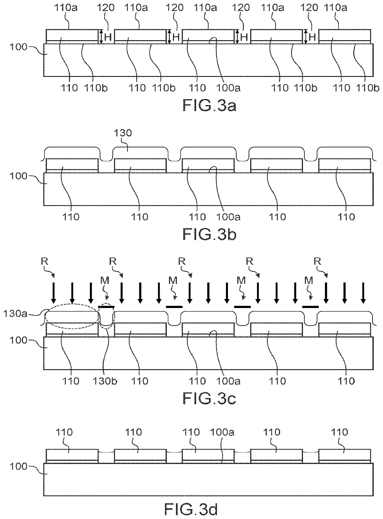
[0021]The purposes of the present invention are, at least in part, achieved by a method for coating chips resting, by a rear face opposite to a front face, on a main face of a substrate, and separated from each other by an inter-chip space, the method comprising the following steps:[0022]a) a step of forming a photosensitive coating film covering the front faces and the inter-chip spaces,[0023]b) a first photolithographic sequence which comprises an insolation sub-step b1), and a dissolution sub-step b2), said sequence leading to a partial removal of the photosensitive coating film so as to maintain said film exclusively at the inter-chip spaces and, advantageously flush or recessed relative to the front faces.

[0024]It is understood, without it being necessary to specify it, that as soon as the chips rest on the main face of the support substrate, said chips are projecting relative to said main face.

[0025]In other words, the inter-chip space formed at the main face and between the c...


PUM


Abstract

A method for coating chips resting, by a rear face opposite to a front face, on a main face of a support substrate, and separated from each other by an inter-chip space, includes a step of forming a photosensitive coating film covering the front faces and the inter-chip spaces. The method further includes a first photolithographic sequence which comprises an insolation sub-step, and a dissolution sub-step. The sequence leads to a partial removal of the photosensitive coating film so as to maintain the film exclusively at the inter-chip spaces and, advantageously recessed relative to the front faces.

Description

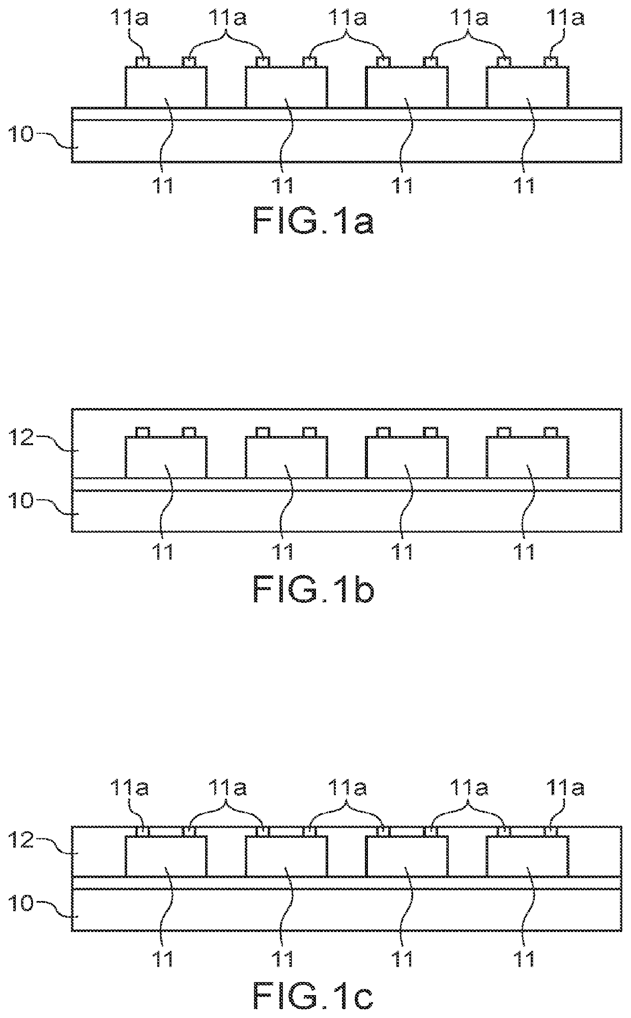
TECHNICAL FIELD[0001]The invention relates to a method for coating chips transferred onto a support substrate. Particularly, the present invention relates to a method for coating chips allowing the integrity, for example the mechanical integrity, of said chips to be preserved.[0002]In particular, the method according to the present invention is advantageously implemented for coating chips having a mechanical fragility with regard to the methods known from the prior art.PRIOR ART[0003]A chip coating method known from the prior art is illustrated in Figures 1a to 1d. [0004]The coating method comprises a first step (FIG. 1a) of assembling the chips 11 on a main face of the support substrate 10. Particularly, the chips are assembled on the main face of the support by their rear face, opposite their front face, and are spaced from each other by spaces, called inter-chip spaces.[0005]A second step, illustrated in FIG. 1b, comprises forming a coating film 12 for the chips, covering the fro...

Claims


Application Information

Patent Timeline
IPC IPC(8): H01L33/44G03F7/16G03F7/11
CPCH01L33/44G03F7/11G03F7/162H01L21/56H01L21/561H01L23/3185H01L25/0657H01L25/18H01L2224/96
Inventor SUHM, AURÉLIENARGOUD, MAXIME
Owner COMMISSARIAT A LENERGIE ATOMIQUE ET AUX ENERGIES ALTERNATIVES
Learn More