
Electronic device and grounding assembly thereof

a technology of electromechanical devices and grounding assemblies, which is applied in the direction of connection contact material, cross-talk/noise/interference reduction, and casings/cabinets/drawers of electrical apparatus, etc., which can solve the problems of difficult to ensure the stability and safety of products, waste of production time, and difficult to ensure product quality

Pending Publication Date: 2022-08-04
DELTA ELECTRONICS INC
View PDF27 Cites 0 Cited by
  • Summary
  • Abstract
  • Description
  • Claims
  • Application Information

AI Technical Summary

Benefits of technology

The present disclosure relates to an electronic device with a grounding assembly. The aim is to provide a safe and stable electronic device by performing the grounding protection procedure after machine assembly and testing without opening the cover of the device. The grounding assembly includes a conducting terminal, a first grounding element, and a second grounding element. The second grounding element sequentially penetrates through the first through hole of the casing, the circuit board, and the conducting terminal, and locks on and electrically couples with the circuit board and the conducting terminal, completing the grounding protection procedure. This invention improves the efficiency of assembly processes, reduces production time and cost, and ensures product quality.

Problems solved by technology

However, it is difficult to ensure the stability and safety of the products during the last two processes.
Moreover, since the assembly process is complicated, it leads waste of production time, and the product quality is also hard to be ensured.

Method used


Image

  • Electronic device and grounding assembly thereof
  • Electronic device and grounding assembly thereof
  • Electronic device and grounding assembly thereof

Examples


Embodiment Construction

[0029]The present invention will now be described more specifically with reference to the following embodiments. It is to be noted that the following descriptions of preferred embodiments of this invention are presented herein for purpose of illustration and description only. It is not intended to be exhaustive or to be limited to the precise form disclosed.

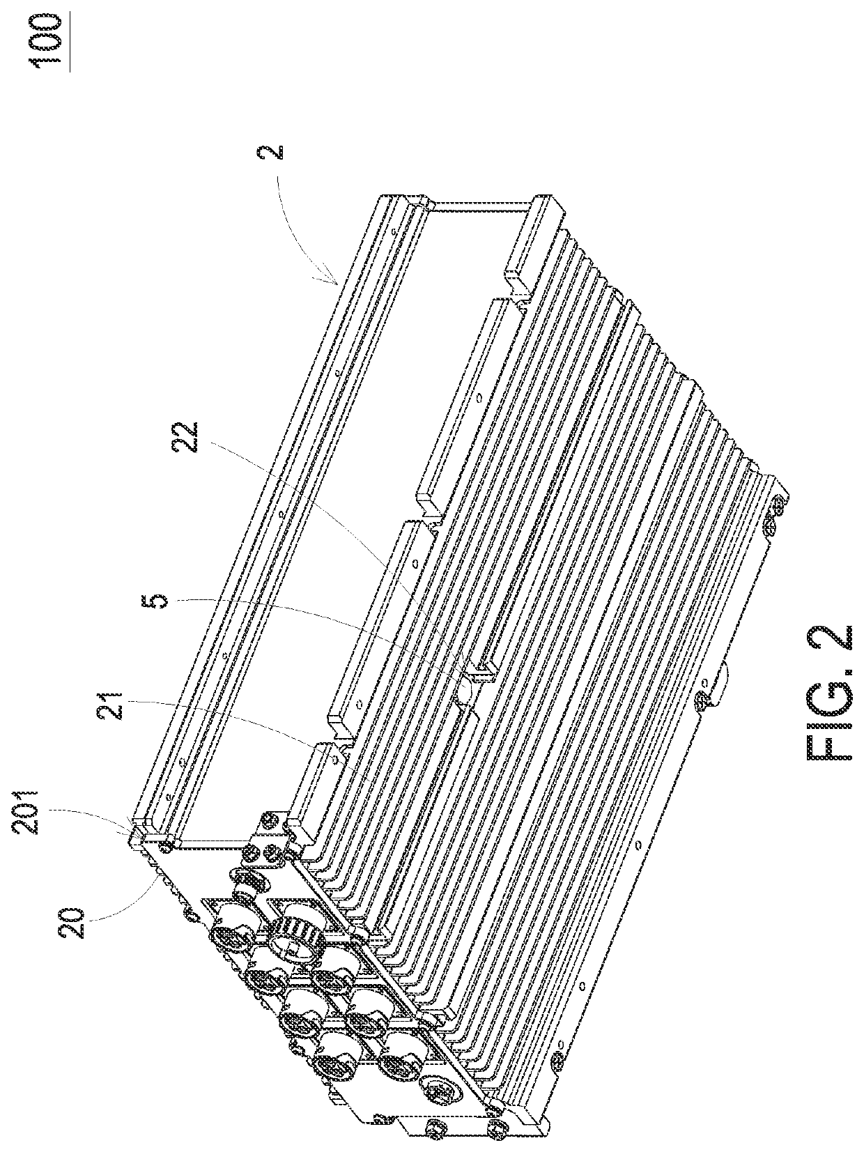
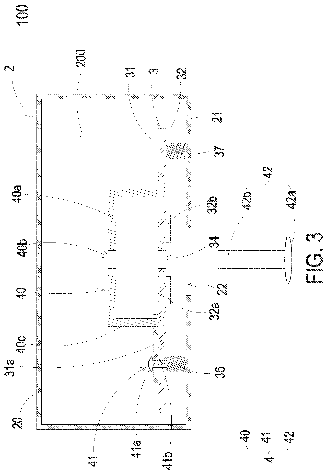
[0030]FIG. 2 is a schematic perspective view illustrating an electronic device according to an embodiment of the present disclosure. FIG. 3 is a schematic cross-sectional view illustrating the electronic device before a Hi-pot test. FIG. 4 is a schematic cross-sectional view illustrating the electronic device after a Hi-pot test. As shown in FIGS. 2-4, the electronic device 100 of the embodiment includes a casing 2, a circuit board 3 and a grounding assembly 4. The casing 2 has a receiving space 200, and the circuit board 3 is disposed within the receiving space 200. The circuit board 3 has a first surface 31 and a second surface...


PUM


Abstract

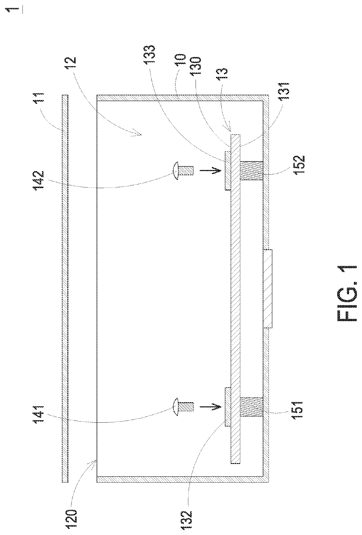
An electronic device includes a casing, a circuit board and a grounding assembly. The circuit board has a first surface and a second surface, wherein an input terminal and an output terminal are disposed on the second surface. The grounding assembly comprises a conducting terminal, a first grounding element and a second grounding element. The conducting terminal is disposed on the first surface of the circuit board, and the first grounding element is disposed adjacent to the conducting terminal. The first grounding element penetrates the circuit board and electrically couples with the conducting terminal and the casing, and the second grounding element correspondingly penetrates the circuit board and the conducting element, so that a first portion of the second grounding element electrically couples with the input terminal and the output terminal of the circuit board, and a second portion of the second grounding element electrically couples with the conducting terminal.

Description

CROSS-REFERENCE TO RELATED APPLICATION[0001]This application claims priority to China Patent Application No. 202110144767.1, filed on Feb. 2, 2021. The entire contents of the above-mentioned applications are incorporated herein by reference for all purposes.FIELD OF THE INVENTION[0002]The present disclosure relates to a grounding assembly, and more particularly to an electronic device and grounding assembly thereof for utilizing in a closed electronic device and can be conducted a high potential test after machine assembly.BACKGROUND OF THE INVENTION[0003]With the rapid development of technology, there are various electronic products developed day by day, these electronic products occupy most of people's daily life. However, in the various electronic products, it is necessary to use the power supply device to convert the AC power into a DC power for the operation of the electronic products.[0004]Especially in the design of the outdoor electronic products, in order to avoid high-volt...

Claims


Application Information

Patent Timeline
Patent Type & Authority Applications(United States)
IPC IPC(8): H05K1/02H05K3/30H05K5/00
CPCH05K1/0215H05K5/006H05K3/301H05K5/0217H05K5/0247H05K7/14H01R4/64H05K2201/10409H05K9/0039
Inventor CHU, CHIA-HSIENCHANG, YI-HUA
Owner DELTA ELECTRONICS INC
Learn More