Heat dissipation structure, semiconductor packaging device, and manufacturing method of the semiconductor packaging device

Active Publication Date: 2022-08-18
GLOBAL UNICHIP CORPORATION +1
View PDF3 Cites 0 Cited by
  • Summary
  • Abstract
  • Description
  • Claims
  • Application Information

AI Technical Summary

Benefits of technology

The invention improves the heat transfer between the chip and the metal lid, making the device better at dissipating heat. As a result, the device's thermal resistance is reduced and its heat dissipation performance is improved.

Problems solved by technology

However, the thermal conductivity of thermally-conductive materials commonly used in the semiconductor package modules is not high, so that the heat dissipation performance of related packages cannot be effectively improved.
If there is no decent heat dissipation technologies for effectively removing the heat energy of the semiconductor package modules, the overall stability and product life of the semiconductor package module will be reduced.
Therefore, the above-mentioned method still has inconveniences and shortcomings, which needs to be further improved.

Method used


Image

  • Heat dissipation structure, semiconductor packaging device, and manufacturing method of the semiconductor packaging device
  • Heat dissipation structure, semiconductor packaging device, and manufacturing method of the semiconductor packaging device
  • Heat dissipation structure, semiconductor packaging device, and manufacturing method of the semiconductor packaging device

Examples


Embodiment Construction

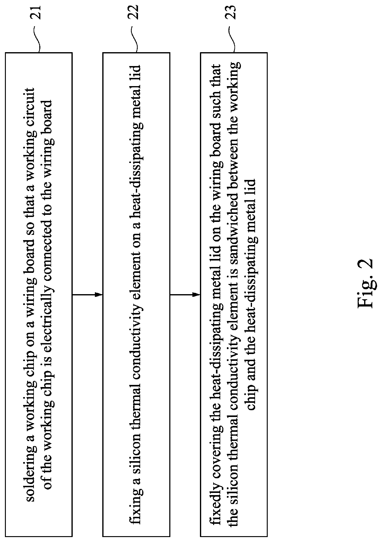
[0020]Reference will now be made in detail to the present embodiments of the present disclosure, examples of which are illustrated in the accompanying drawings. Wherever possible, the same reference numbers are used in the drawings and the description to refer to the same or like parts. According to the embodiments, it will be apparent to those skilled in the art that various modifications and variations can be made to the structure of the present disclosure without departing from the scope or spirit of the present disclosure.

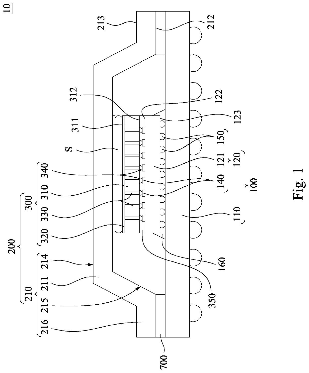
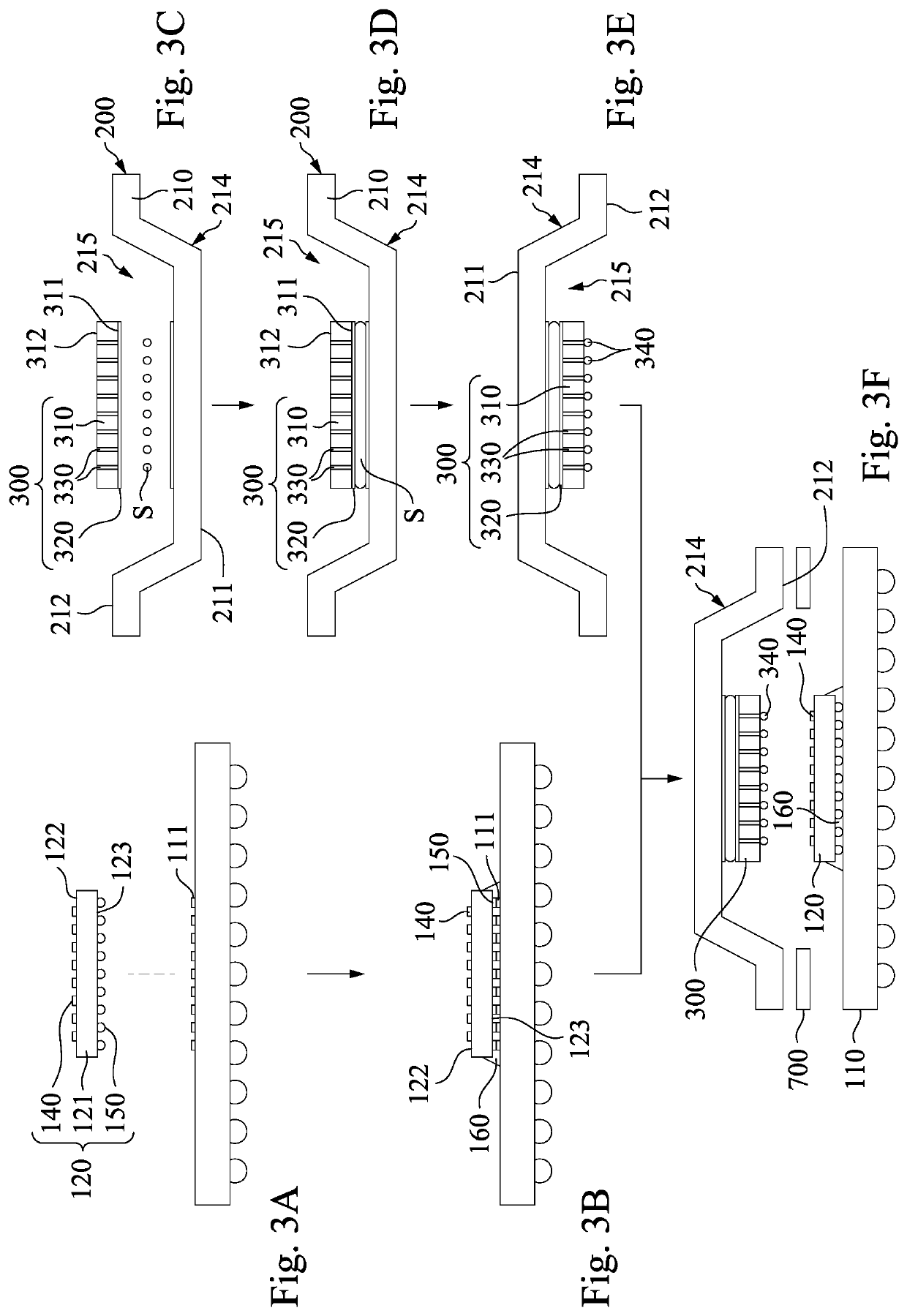
[0021]Reference is now made to FIG. 1, in which FIG. 1 is a schematic view of a semiconductor packaging device 10 according to one embodiment of the present disclosure. As shown in FIG. 1, the semiconductor packaging device 10 includes a heat source 100 and a heat dissipation structure 200. The heat dissipation structure 200 is used to remove high heat energy of the heat source 100. The heat source 100 includes a wiring board 110 and a working chip 120 (e.g., s...


PUM


Abstract

A semiconductor packaging device includes a wiring board, a working chip, a heat-dissipating metal lid and a silicon thermal conductivity element. The working chip is mounted on the wiring board, and in-built with an working circuit therein. The silicon thermal conductivity element is thermally coupled to the working chip and the heat-dissipating metal lid, and is electrically isolated from the working circuit and the wiring board.

Description

RELATED APPLICATIONS[0001]This application claims priority to Taiwan Application Serial Number 110105549, filed on Feb. 18, 2021, which is herein incorporated by reference.BACKGROUNDField of Disclosure[0002]The present disclosure relates to a heat dissipation structure, a semiconductor packaging device, and a manufacturing method of the semiconductor packaging device.Description of Related Art[0003]As the volume of the semiconductor package modules starts to be miniaturized, the performance of the semiconductor package module is continuously enhanced, and with the higher heat generation, suitable heat dissipation technologies are required to effectively dissipate the heat.[0004]However, the thermal conductivity of thermally-conductive materials commonly used in the semiconductor package modules is not high, so that the heat dissipation performance of related packages cannot be effectively improved. If there is no decent heat dissipation technologies for effectively removing the heat...

Claims


Application Information

Patent Timeline
IPC IPC(8): H01L23/367H01L21/48H01L23/31H01L21/56H01L23/00H01L23/373
CPCH01L23/3675H01L2224/73253H01L23/3185H01L21/563H01L24/92H01L24/16H01L24/33H01L24/32H01L24/73H01L24/13H01L24/17H01L23/3735H01L23/3192H01L2924/10253H01L2224/16145H01L2224/92125H01L2224/33181H01L2224/17181H01L2224/13025H01L24/81H01L2224/92225H01L2224/81815H01L2924/10272H01L2224/92242H01L2224/73204H01L2224/33519H01L2224/32145H01L2224/17519H01L21/4882H01L23/433H01L23/3738H01L23/3677H01L23/053H01L21/4817H01L21/56H01L23/3128H01L2224/16225H01L2224/32225
Inventor CHEN, JIA-LIANGYANG, CHI-MINGLIN, YEN-CHAO
Owner GLOBAL UNICHIP CORPORATION
Why Eureka
Try Eureka