Wafer inspection system

a technology of wafers and inspection systems, applied in the direction of electronic circuit testing, measurement devices, instruments, etc., can solve the problems of easy control, increased cost, and liable temperature of the supporting unit of the conductor uni

Active Publication Date: 2022-09-22
MPI CORP
View PDF5 Cites 0 Cited by
  • Summary
  • Abstract
  • Description
  • Claims
  • Application Information

AI Technical Summary

Benefits of technology

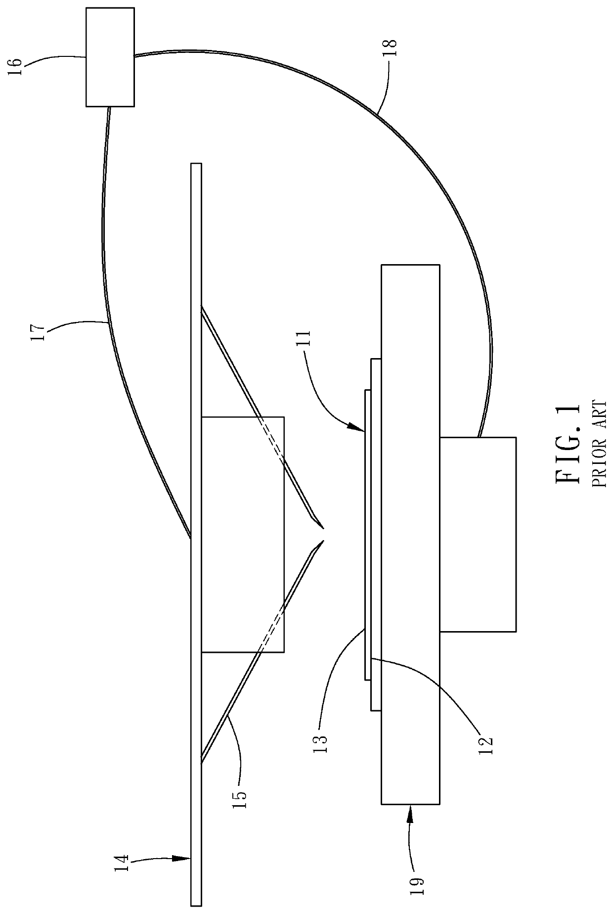
[0005]However, for the die inspections under specific temperature conditions, the temperature of the above-described supporting unit for supporting the wafer will be adjusted by a temperature control device, which means the temperature of the supporting unit may be raised or lowered. Therefore, the conducting units disposed on the supporting unit are liable to be affected by the temperature of the supporting unit, e.g. thermal expansion and contraction caused by temperature changes. In order to improve this situation, the configuration of the conducting units will be more complicated, such as provided with thermal insulation members, thereby increasing the cost. The above-described thermal expansion and contraction will also cause the unstable performance of the conducting units, resulting in that the contact stability thereof is not easy to be controlled, thereby affecting the stability of the test signal transmission. Besides, the above-described probing process is usually performed in a way that the wafer is moved upwardly by the supporting unit to make the die contacted by the probe. In addition, the conducting unit is usually an elastic contact member (pogo pin) provided with a spring and a contact head. In order for the spring to bear the weight of the contact head and to elastically push the contact head to cause good contact between the contact head and the electrically conductive portion of the probe device to provide stable test signal, the spring constant (K-value) of the conducting unit will be provided higher. As such, the load of the vertical movement of the supporting unit may be increased, especially in the condition with relatively more conducting units. Furthermore, as shown in FIG. 10 of the aforementioned patent (the reference numerals used below are given accordingly to the associated reference numerals used in the figures of the patent), when the outermost die of the wafer is contacted by the probe, the conducting unit 210 is abutted against the innermost side of the electrically conductive portion 320 of the probe device. Under this circumstance, if the wafer is placed with a little positional deviation, such as slightly deviated to the left, in order to make the detection part 310 contact the outermost (the leftmost) die of the wafer, the conducting unit 210 may have to be moved to the edge of the electrically conductive portion 320 located between the electrically conductive portion 320 and the probe (the detection part 310), resulting in partial contact of a single conducting unit 210 or even non-contact of partial conducting units 210, thereby undesirably decreasing the contact area, which in turn affecting the stability of the test signal transmission.
[0006]The present invention has been accomplished in view of the above-noted circumstances. It is an objective of the present invention to provide a wafer inspection system, which can satisfy the test requirement of short-pulse test signal and prevent the structural design and transmission stability of test signal transmitting members from being affected by the inspection temperature.

Problems solved by technology

Therefore, the conducting units disposed on the supporting unit are liable to be affected by the temperature of the supporting unit, e.g. thermal expansion and contraction caused by temperature changes.
In order to improve this situation, the configuration of the conducting units will be more complicated, such as provided with thermal insulation members, thereby increasing the cost.
The above-described thermal expansion and contraction will also cause the unstable performance of the conducting units, resulting in that the contact stability thereof is not easy to be controlled, thereby affecting the stability of the test signal transmission.

Method used


Image

  • Wafer inspection system
  • Wafer inspection system
  • Wafer inspection system

Examples


Embodiment Construction

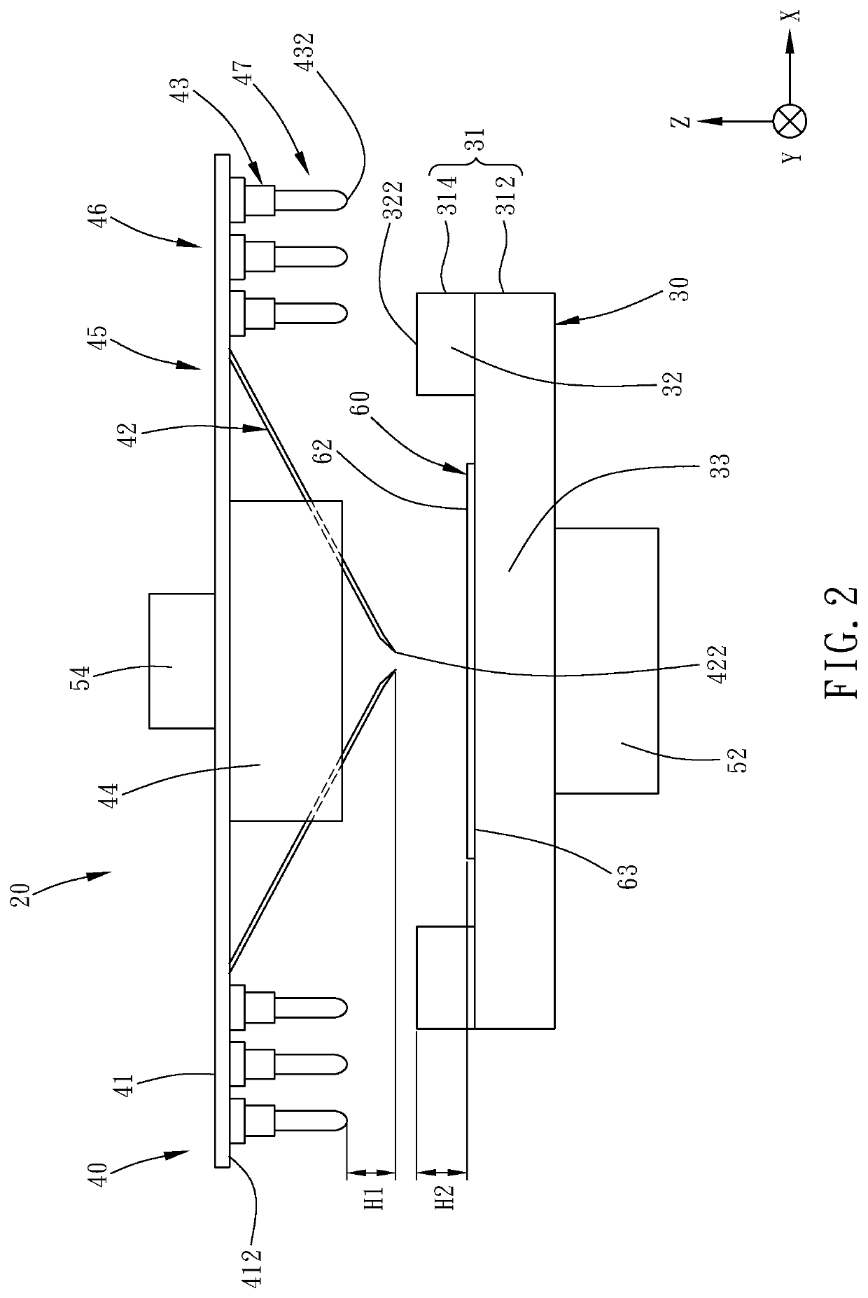
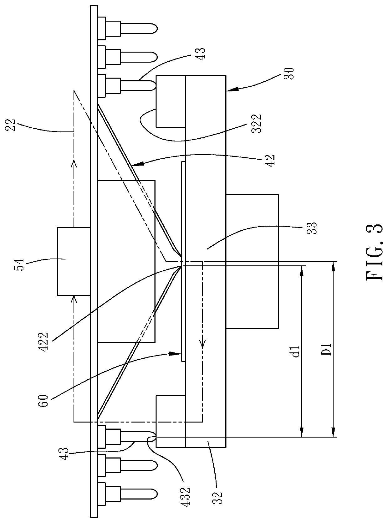
[0027]First of all, it is to be mentioned that same reference numerals used in the following embodiments and the appendix drawings designate same or similar elements or the structural features thereof throughout the specification for the purpose of concise illustration of the present invention. It should be noticed that for the convenience of illustration, the components and the structure shown in the figures are not drawn according to the actual dimensions and numbers, and the features mentioned in one embodiment can be applied in the other embodiments if it can be accomplished. Besides, when it is mentioned that an element is disposed on another element, it means that the former element is directly disposed on the latter element, or the former element is indirectly disposed on the latter element through one or more other elements between the aforesaid former and latter elements. When it is mentioned that an element is directly disposed on another element, it means that no other el...


PUM


Abstract

A wafer inspection system includes a supporting device having electrically connected supporting and contact portions for supporting a wafer's back, and a probe device having a probe and elastic contact members. When a probe tip of the probe contacts the wafer's front, a contact tip of the elastic contact member is abutted against a contact surface of the contact portion. The contact tip is higher than the probe tip. The contact surface is higher than the wafer's front. Alternatively, the contact surface having a radius larger than or equal to twice the wafer's radius. The horizontal distance between the probe tip and the contact tip is larger than or equal to twice the wafer's radius. This satisfies the test requirement of short-pulse test signal and prevents the structural design and transmitting stability of the elastic contact members from being affected by the inspection temperature.

Description

BACKGROUND OF THE INVENTION1. Field of the Invention[0001]The present invention relates generally to wafer inspection systems and more particularly, to a wafer inspection system which is provided around the outer periphery of probes of a probe device thereof with elastic contact members for being electrically connected with the negative electrode of a wafer.2. Description of the Related Art[0002]Referring to FIG. 1, it is well known that a vertical type die refers to a die provided with a positive contact and a negative contact respectively on the front and back thereof. For example, the back 12 of a wafer 11 may serve as a common plane negative contact of all dies of the wafer 11. The vertical type die is usually a light emitting die, such as VCSEL, micro LED, mini LED, and so on and the light emitting portion thereof is located on the front 13 of the wafer 11. As regards the probing of the above-described vertical type die, the positive electrode of the die, i.e. the front of the ...

Claims


Application Information

Patent Timeline
Patent Type & Authority Applications(United States)
IPC IPC(8): G01R31/28G01R1/067G01R1/073
CPCG01R31/2865G01R1/06727G01R1/07392G01R31/2601G01R31/2637G01R1/0408G01R1/07307G01R1/07342G01R31/2889
Inventor CHENG, YI-HSUANLIN, HUNG-IPENG, PO-HAN
Owner MPI CORP
Why Eureka
Try Eureka