Unlock instant, AI-driven research and patent intelligence for your innovation.

Shaped aperture set for multi-beam array configurations

a technology of aperture array and configuration, applied in the field of multi-beam array system, can solve the problems of increasing inspection system cost, requiring additional maintenance, and not being able to detect defects of decreasing siz

Active Publication Date: 2022-09-29
KLA TENCOR TECH CORP
View PDF7 Cites 0 Cited by
  • Summary
  • Abstract
  • Description
  • Claims
  • Application Information

AI Technical Summary

Benefits of technology

The present patent provides an aperture array for a multi-beam array system. The array body has a plurality of apertures, which can be moved relative to the beam source to select a subset of the beam. The apertures can have different geometries, such as circular, rectangular, hexagonal, or other shapes. The actuator can move the array body in an X or Y direction, or in both directions, and can be a linear or rotary actuator. The aperture array can be made of materials such as aluminum nitride, polycrystalline diamond, graphite, molybdenum, or tungsten. The distance between the array body and the beam source can be from 10 cm to 20 cm. The method of selecting a beam can involve directing the electron beam through the array body and selecting the desired portion of the wafer based on the shape of the aperture intersected by the optical axis. The technical effects of the invention include improved precision in selecting a beam and improved efficiency in processing wafers.

Problems solved by technology

However, as the dimensions of semiconductor devices decrease, inspection becomes even more important to the successful manufacture of acceptable semiconductor devices because smaller defects can cause the devices to fail.
For instance, as the dimensions of semiconductor devices decrease, detection of defects of decreasing size has become necessary because even relatively small defects may cause unwanted aberrations in the semiconductor devices.
These methods can add cost to the inspection system and / or can require additional maintenance.

Method used


Image

  • Shaped aperture set for multi-beam array configurations
  • Shaped aperture set for multi-beam array configurations
  • Shaped aperture set for multi-beam array configurations

Examples


Embodiment Construction

[0037]Although claimed subject matter will be described in terms of certain embodiments, other embodiments, including embodiments that do not provide all of the benefits and features set forth herein, are also within the scope of this disclosure. Various structural, logical, process step, and electronic changes may be made without departing from the scope of the disclosure. Accordingly, the scope of the disclosure is defined only by reference to the appended claims.

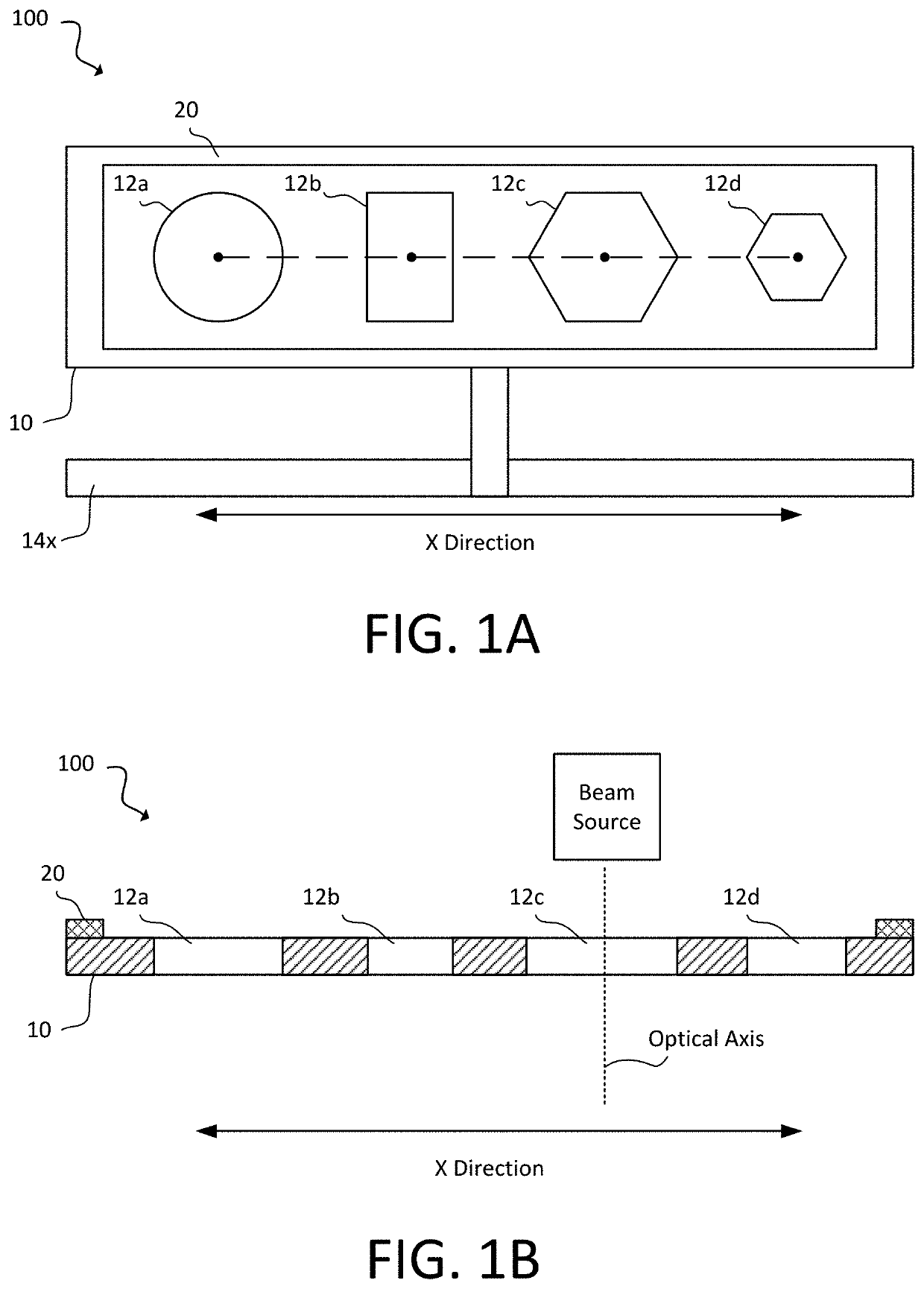
[0038]As shown in FIG. 1A, an embodiment of the present disclosure provides an aperture array 100 for a multi-beam array system. The aperture array 100 may comprise an array body 10. The array body 10 may be a plate having a thickness of at least 100 μm. The array body 10 may be comprised of one of the following materials: aluminum nitride, polycrystalline diamond, graphite, molybdenum, and tungsten. Other materials are possible and these materials are merely listed as examples.

[0039]The array body 10 may comprise a plura...


PUM


Abstract

An aperture array for a multi-beam array system and a method of selecting a subset of a beam from a multi-beam array system are provided. The aperture array comprises an array body arranged proximate to a beam source. The array body comprises a plurality of apertures, at least two of the apertures having different geometries. The array body is movable, via an actuator, relative to an optical axis of the beam source, such that a subset of a beam from the beam source is selected based on the geometry of the aperture that is intersected by the optical axis.

Description

FIELD OF THE DISCLOSURE[0001]This disclosure relates to a multi-beam array system and, more particularly, to an aperture array for a multi-beam array system.BACKGROUND OF THE DISCLOSURE[0002]Evolution of the semiconductor manufacturing industry is placing greater demands on yield management and, in particular, on metrology and inspection systems. Critical dimensions continue to shrink, yet the industry needs to decrease time for achieving high-yield, high-value production. Minimizing the total time from detecting a yield problem to fixing it determines the return-on-investment for a semiconductor manufacturer.[0003]Fabricating semiconductor devices, such as logic and memory devices, typically includes processing a semiconductor wafer using a large number of fabrication processes to form various features and multiple levels of the semiconductor devices. For example, lithography is a semiconductor fabrication process that involves transferring a pattern from a reticle to a photoresist...

Claims


Application Information

Patent Timeline
IPC IPC(8): H01J37/22G01N23/2251
CPCH01J37/226G01N23/2251H01J37/28H01J2237/0458H01J37/09H01J2237/0451G01N2223/6116G01N2223/646
Inventor PLETTNER, TOMASESCORCIA, ERNESTOSHRIYAN, SAMEET K.LEE, JEONG HO
Owner KLA TENCOR TECH CORP