Photoelectric conversion device

Pending Publication Date: 2022-11-03
CANON KK
View PDF0 Cites 0 Cited by
  • Summary
  • Abstract
  • Description
  • Claims
  • Application Information

AI Technical Summary

Benefits of technology

The patent text describes a technique to improve the flexibility of setting exposure time in a photoelectric device that includes a pixel with multiple photoelectric converters. The technique involves sharing one floating diffusion among the converters. The technical effect of this invention is to enhance the performance of the photoelectric conversion device.

Problems solved by technology

Therefore, the degree of freedom in setting the exposure time of the photoelectric converter is not necessarily high.

Method used


Image

  • Photoelectric conversion device
  • Photoelectric conversion device
  • Photoelectric conversion device

Examples


first embodiment

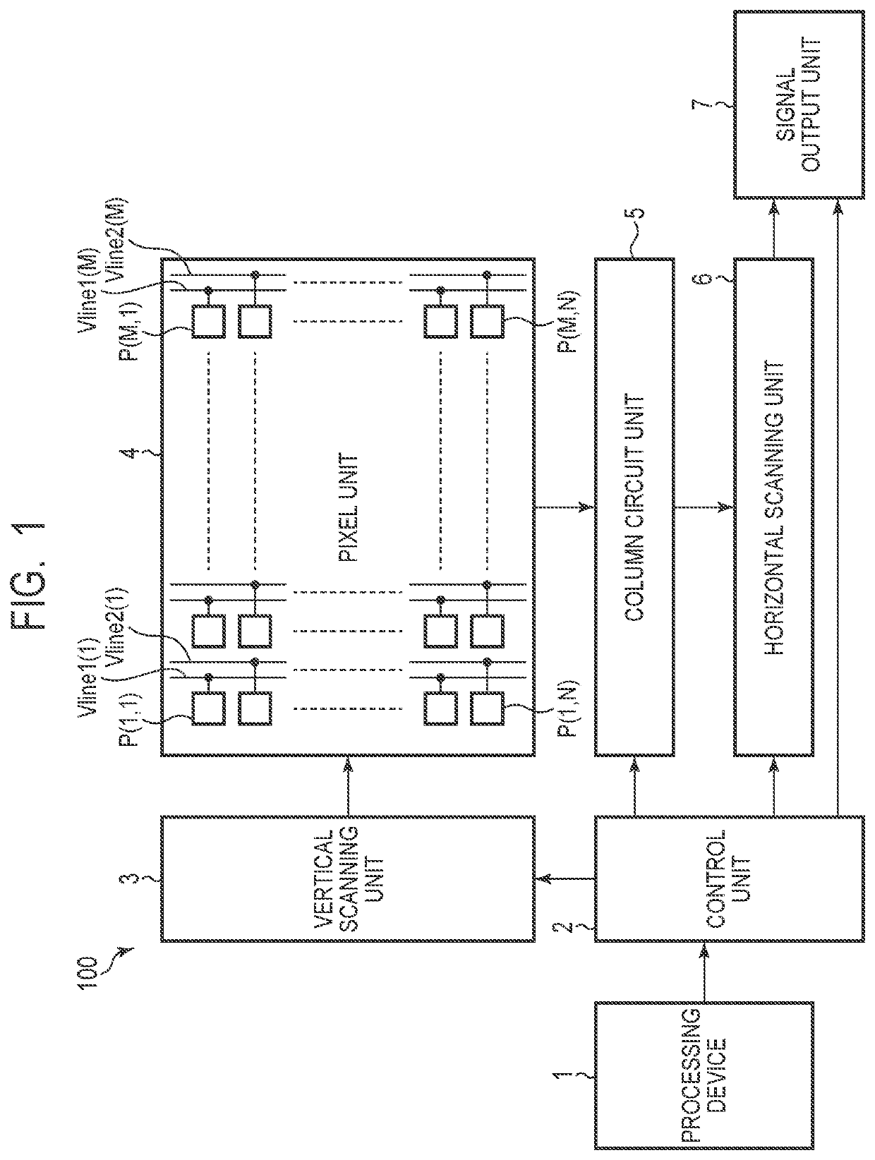
[0031]A schematic configuration of a photoelectric conversion device according to a first embodiment of the present invention will be described with reference to FIG. 1. FIG. 1 is a block diagram illustrating a schematic configuration of a photoelectric conversion device according to the present embodiment.

[0032]As illustrated in FIG. 1, for example, the photoelectric conversion device 100 according to the present embodiment may include a processing device (processor) 1, a control unit 2, a vertical scanning unit 3, a pixel unit 4, a column circuit unit 5, a horizontal scanning unit 6, and a signal output unit 7. The vertical scanning unit 3 and the column circuit unit 5 are connected to the pixel unit 4. A horizontal scanning unit 6 is connected to the column circuit unit 5. A signal output unit 7 is connected to the horizontal scanning unit 6. A control unit 2 is connected to the vertical scanning unit 3, the column circuit unit 5, the horizontal scanning unit 6, and the signal ou...

second embodiment

[0151]A photoelectric conversion device according to a second embodiment of the present invention will be described with reference to FIG. 10 to FIG. 12. The same components as those of the photoelectric conversion device according to the first embodiment are denoted by the same reference numerals, and the description thereof will be omitted or simplified.

[0152]The photoelectric conversion device according to the present embodiment is different from the photoelectric conversion device according to the first embodiment in the configuration of a counter that counts the horizontal synchronization signal Hpd.

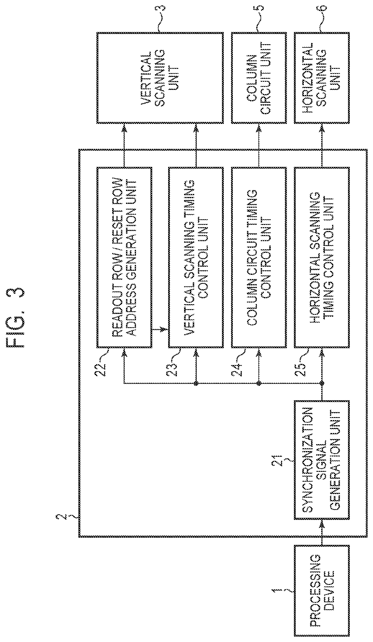
[0153]First, a configuration example of the readout row / reset row address generation unit 22 in the photoelectric conversion device according to the present embodiment will be described with reference to FIG. 10. FIG. 10 is a block diagram illustrating a configuration example of a readout row / reset row address generation unit 22 in the photoelectric conversion device according to th...

third embodiment

[0193]A photoelectric conversion device according to a third embodiment of the present invention will be described with reference to FIG. 13 to FIG. 14. The same components as those of the photoelectric conversion devices according to the first and second embodiments are denoted by the same reference numerals, and the description thereof will be omitted or simplified.

[0194]The photoelectric conversion device according to the present embodiment is different from the photoelectric conversion device according to the first embodiment in the configuration of a counter that counts the horizontal synchronization signal Hpd.

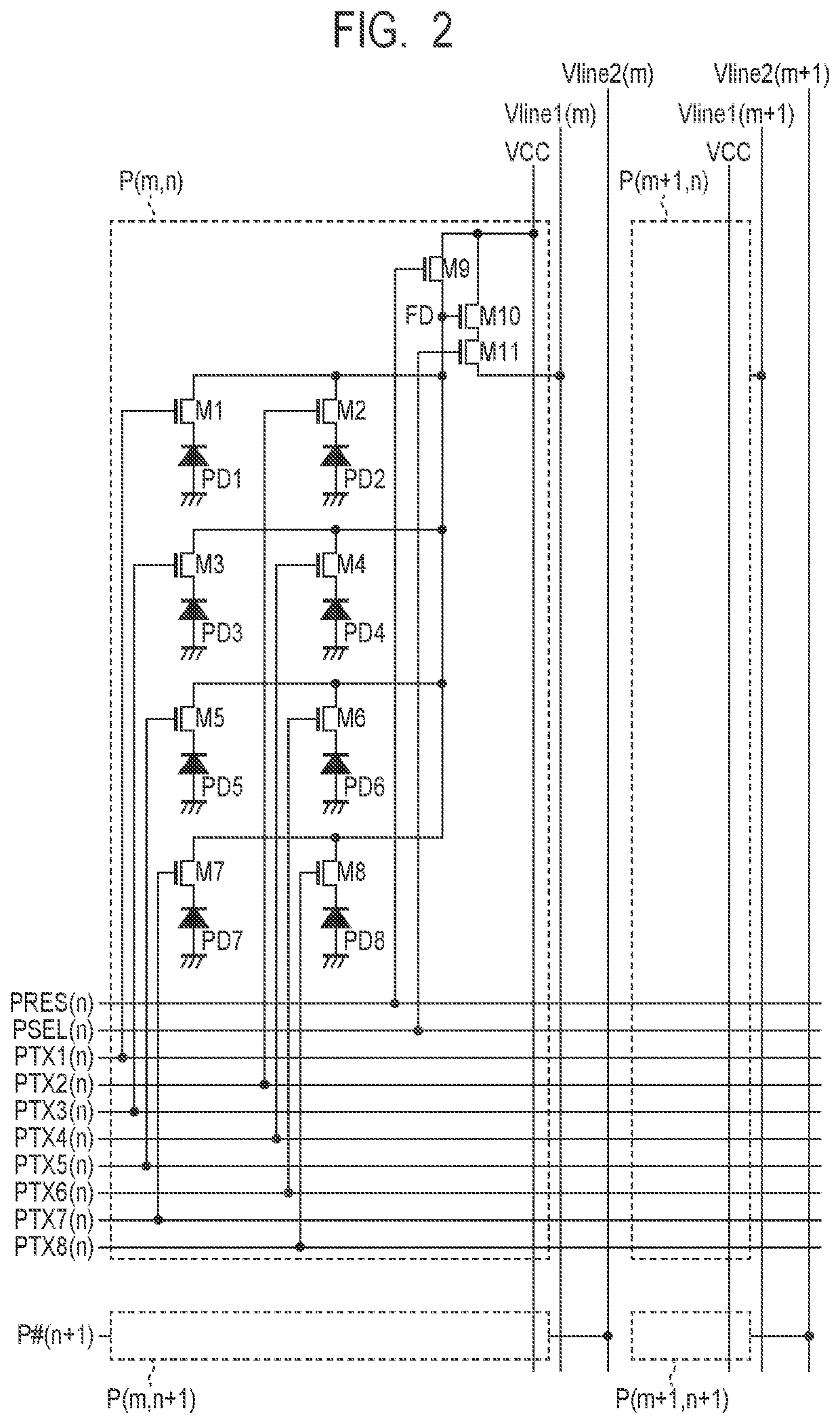
[0195]First, a configuration example of the pixel P in the photoelectric conversion device according to the present embodiment will be described with reference to FIG. 13. FIG. 13 is a circuit diagram illustrating a configuration example of a pixel P in the photoelectric conversion device according to the present embodiment. FIG. 13 illustrates only the configuration of ...


PUM


Abstract

The photoelectric conversion device includes pixels each including photoelectric converters and a floating diffusion to which charges of the photoelectric converters are transferred, a vertical scanning unit for performing readout processing and reset processing on the pixels while switching the photoelectric converter to be processed and the floating diffusion to be processed, and a control unit that controls the vertical scanning unit. The control unit includes a readout row address generation unit and a reset row address generation unit that generate a row address to be processed. A first cycle in which the photoelectric converter is switched is shorter than a second cycle in which the floating diffusion is switched, an update cycle of the row address is equal to the second cycle, and a setting unit of an update timing of the row address is equal to the length of one cycle of the first cycle.

Description

BACKGROUND OF THE INVENTIONField of the Invention[0001]The present invention relates to a photoelectric conversion device.Description of the Related Art[0002]Japanese Patent Application Laid-Open No. 2013-118698 discloses an image sensor including pixels in which a plurality of photoelectric converters shares one floating diffusion. Japanese Patent Application Laid-Open No. 2008-288946 discloses a method in which pixels on which each process is to be performed are specified one line at a time and each process is performed as a method of reading out charge from a photoelectric converter and resetting the photoelectric converter in a general imaging device.[0003]When the technique described in Japanese Patent Application Laid-Open No. 2008-288946 is applied to Japanese Patent Application Laid-Open No. 2013-118698, while one floating diffusion is selected over a plurality of horizontal periods, a plurality of photoelectric converters sharing the floating diffusion are sequentially sele...

Claims


Application Information

Patent Timeline
IPC IPC(8): H04N5/374H04N5/3745
CPCH04N5/3743H04N5/3742H04N5/37455H04N25/531H04N25/778H04N25/745H04N25/768H04N25/767H04N25/772
Inventor KASUGAI, TAICHITAKENAKA, SHINTARO
Owner CANON KK
Why Eureka
Try Eureka