

Electronic substrate
- Summary
- Abstract
- Description
- Claims
- Application Information
AI Technical Summary
Benefits of technology
Problems solved by technology
Method used
Image

Examples
first embodiment
(1)
(2) Second embodiment:
(3) Third embodiment:
(4) Other embodiments:
(1) First Embodiment
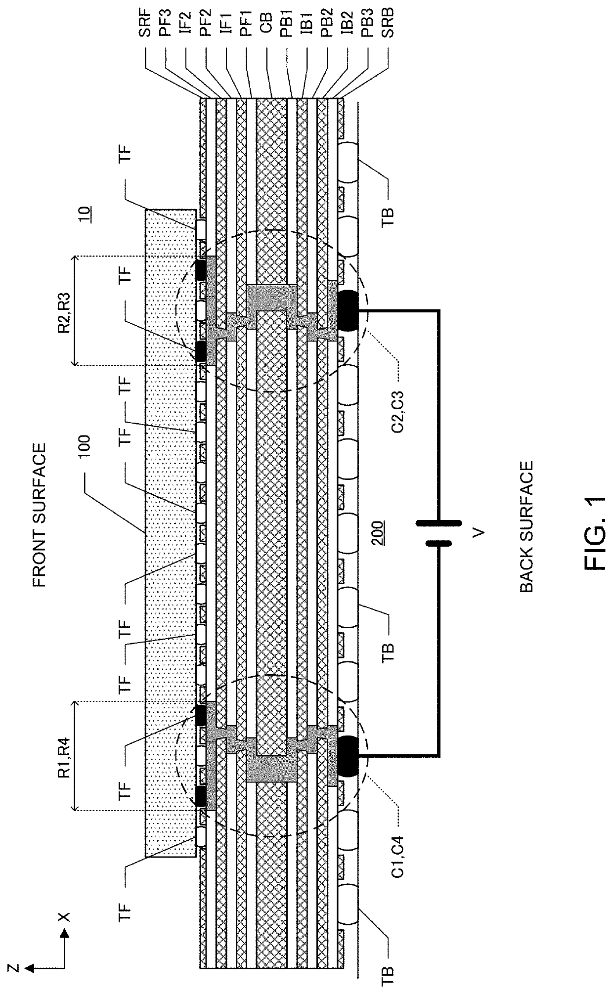
[0013]FIG. 1 is a schematic sectional view of an electronic substrate 10 according to an embodiment of the present disclosure. The electronic substrate 10 is a rectangular plate-shaped other-layer substrate, and a plurality of layers are laminated in the thickness direction Z. One side of the electronic substrate 10 in the thickness direction Z (upper side of the paper surface) is defined as a front surface, and the other side in the thickness direction Z (lower side of the paper surface) is defined as the front surface. The electronic substrate 10 includes six layers of conductor layers PF1, PF2, PF3, PB1, PB2, and PB3 and seven layers of insulating layers CC, IF1, IF2, SRF, IB1, IB2, and SRB. The electronic substrate 10 of the present embodiment is a double-sided build-up substrate in which each layer is laminated on an insulating layer CC which is a core substrate. However, the electronic subs...
second embodiment
(2) Second Embodiment
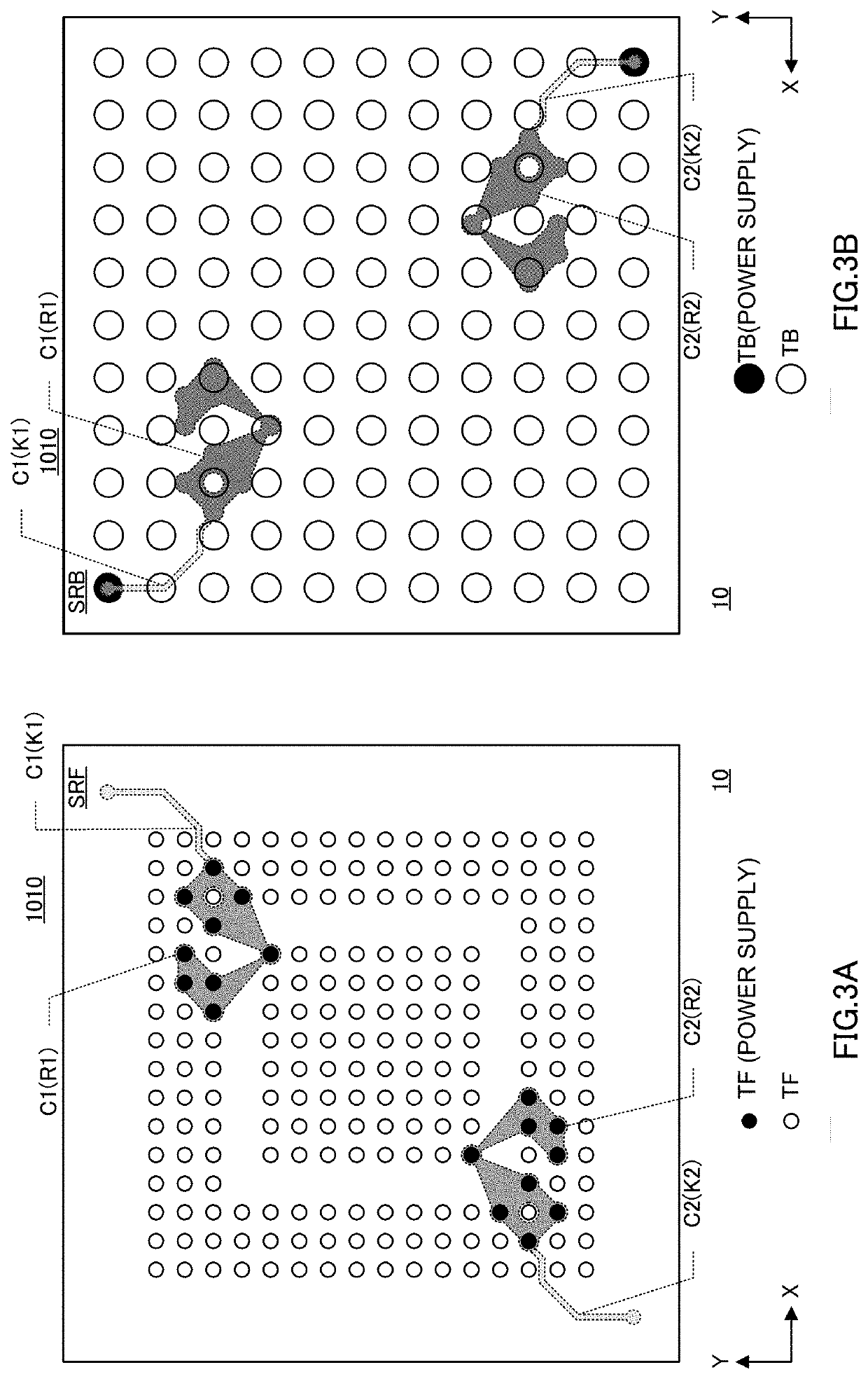
[0037]FIGS. 3A and 3B show the front surface and the back surface of an electronic substrate 1010 according to a second embodiment. Also in the present embodiment, the wiring patterns constituting the first to second wirings C1 to C2 are formed in the conductor layer PF3 on the frontmost surface side. Of the wiring pattern of the conductor layer PF3, a part formed in the portion where the front surface terminals TF (black circles) to which the power supply V is supplied exist is represented by first to second basic regions R1 to R2, and the first to second basic regions R1 to R2 (perspective images) are shown in dark gray. Further, of the wiring pattern of the conductor layer PF3, a part formed in the portion where the front surface terminals TF to which the power supply V is supplied do not exist is represented by first to second expansion regions K1 to K2, and the first to second expansion regions K1 to K2 (perspective images) are shown in light gray.
[0038]The...
third embodiment
(3) Third Embodiment
[0040]FIG. 4 is a schematic sectional view of an electronic substrate 2010 according to a third embodiment. The electronic substrate 2010 is a multi-chip module (MCM) substrate, and a first semiconductor component 100A and a second semiconductor component 100B are mounted on the electronic substrate 2010 on the front surface. The first wiring C1 is connected to both of the front surface terminals TF connected to the first semiconductor component 100A and the front surface terminals TF connected to the second semiconductor component 100B. As a result, the power supply V can be supplied to both of the first semiconductor component 100A and the second semiconductor component 100B via the first wiring C1.
(4) Other Embodiments
[0041]In the above, the electronic substrates 10, 1010, 2010 having the number of wirings connected to the power supply V of four and two are illustrated, but the number of wirings for supplying the power supply V only needs to be two or more. Fu...
PUM
 Abstract
Description
Claims
Application Information