High voltage semiconductor device and method of manufacturing same

a semiconductor and high-voltage technology, applied in the direction of semiconductor devices, basic electric elements, electrical apparatus, etc., can solve the problems of deterioration of the device's on-resistance, difficulty in solving the problem of electric field concentration, etc., to improve the breakdown voltage of the device, reduce or prevent the deterioration of the on-resistance

Pending Publication Date: 2022-11-17
DONGBU HITEK CO LTD
View PDF0 Cites 4 Cited by
  • Summary
  • Abstract
  • Description
  • Claims
  • Application Information

AI Technical Summary

Benefits of technology

[0032]The present disclosure has the following effects by the above configurations.
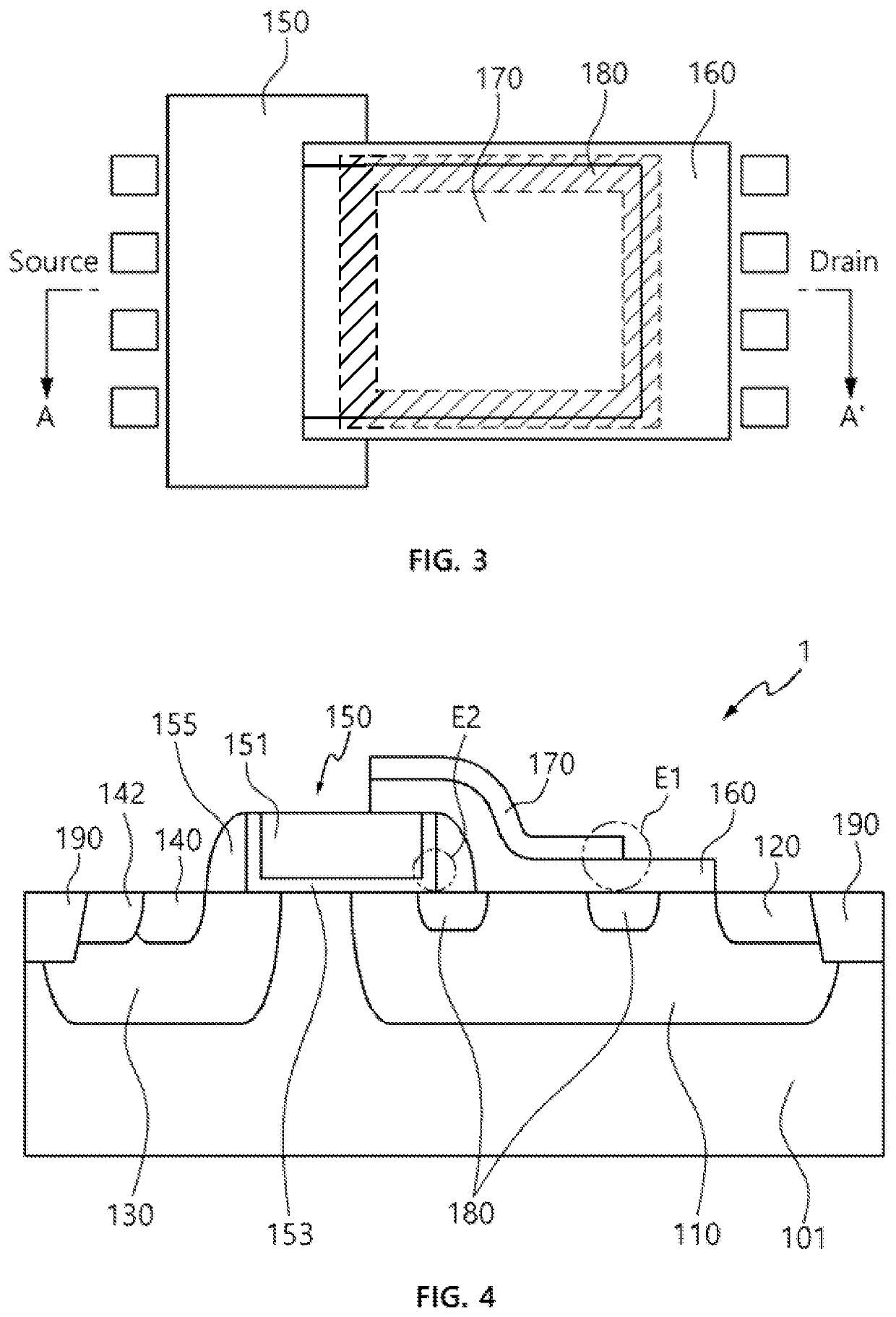
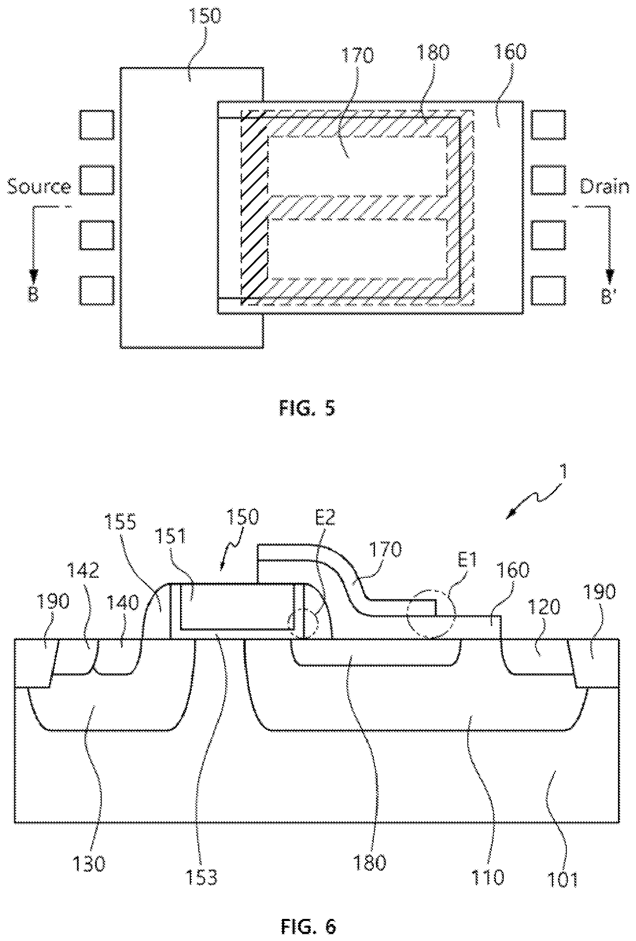
[0033]The present disclosure can reduce or prevent deterioration of the on-resistance as a result of the STI feature intended to prevent electric field concentration caused by a field plate by forming a shallow-depth top region on the surface of a substrate in the high voltage semiconductor device having the field plate.
[0034]In addition, the present disclosure can improve the breakdown voltage of the device while preventing the on-resistance from deteriorating as the top region is below the electric field concentration regions resulting from the field plate, and extends in a first direction and includes an opening providing a current path, thereby reducing or minimizing an increase in the length of the current path due to the formation of the top region.
[0035]Moreover, the present disclosure can improve the on-resistance of the device by providing the top region with a shape that extends along the field plate or a lower edge thereof.
[0036]Furthermore, the present disclosure can enhance the RESURF effect as the top region extends along the field plate and includes a portion or section extending across the field plate along the first direction.
[0037]Meanwhile, it should be added that even if effects are not explicitly mentioned herein, the effects described in the following specification expected by the technical features of the present disclosure and their potential effects are treated as if they were described in the present disclosure.

Problems solved by technology

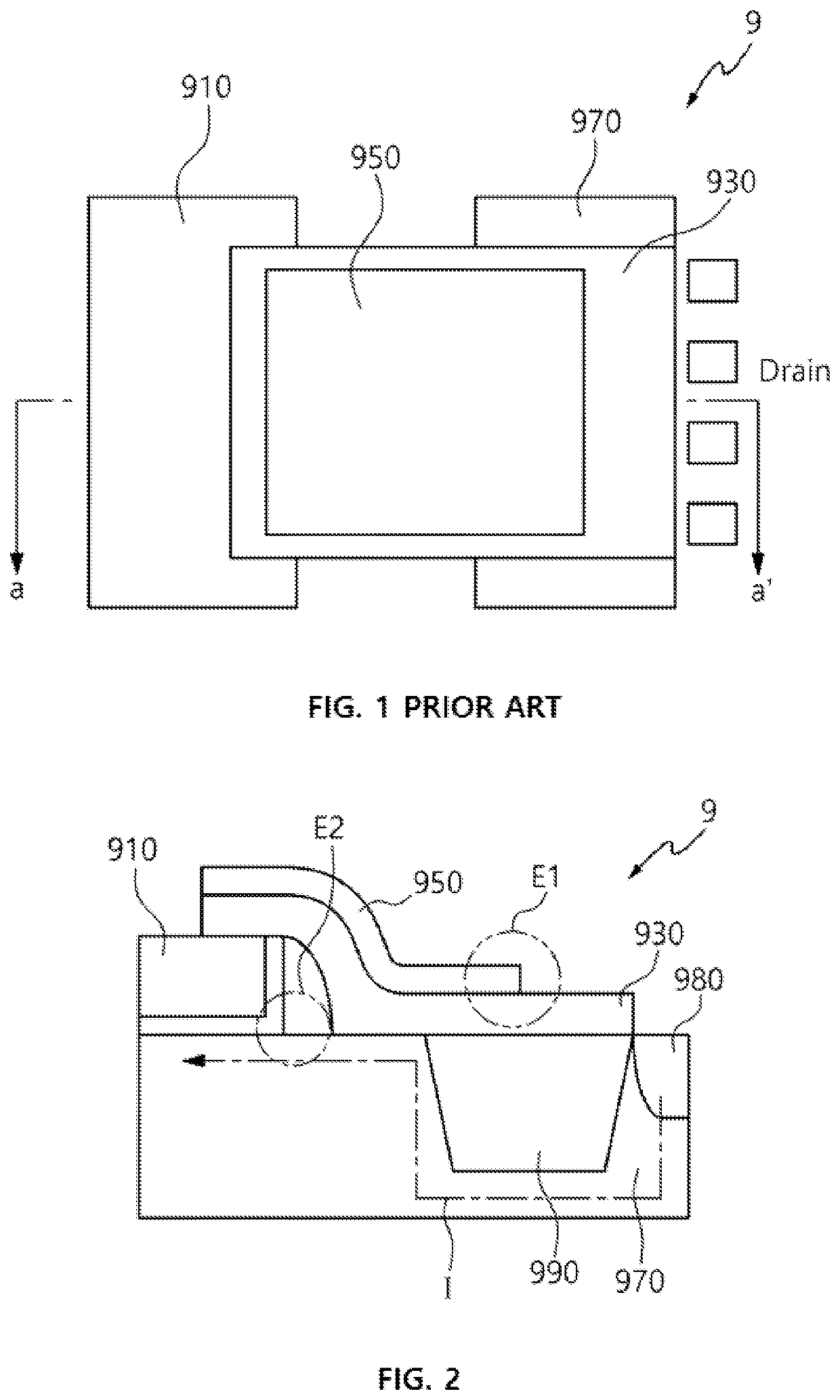
However, there is still a difficulty in solving the electric field concentration problem at the lower end E2 of the gate electrode 910.
In addition, since the STI 990 feature increases the length of a current path I in the drift region 970, the on-resistance of the device inevitably deteriorates as well.

Method used


Image

  • High voltage semiconductor device and method of manufacturing same
  • High voltage semiconductor device and method of manufacturing same
  • High voltage semiconductor device and method of manufacturing same

Examples


Embodiment Construction

[0045]Hereinafter, embodiments of the present disclosure will be described in more detail with reference to the accompanying drawings. The embodiments of the present disclosure may be modified in various forms, and the scope of the present disclosure should not be construed as being limited to the following embodiments, but should be construed based on the claims. In addition, these embodiments are provided for reference in order to more completely explain the present disclosure to those skilled in the art.

[0046]Hereinafter, it should be noted that when one component (or layer) is described as being on another component (or layer), the component may be directly on another component, or one or more third components or layers may be between the one component and the other component. In addition, when one component is expressed as being directly on or above another to component, no other component(s) are located between the one component and the other component. Moreover, the terms “to...


PUM

PropertyMeasurementUnit
insulatingaaaaaaaaaa
conductivityaaaaaaaaaa
concentrationaaaaaaaaaa

Abstract

Disclosed is a high voltage semiconductor device and a method of manufacturing the same and, more particularly, to a high voltage semiconductor device and a method of manufacturing the same that enables an improvement in the breakdown voltage relative to the on-resistance by forming a top region in or at the surface of the substrate when the device includes a field plate adjacent to a gate electrode.

Description

CROSS REFERENCE TO RELATED APPLICATION(S)[0001]The present application claims priority to Korean Patent Application No. 10-2021-0061302, filed on May 21, 2021, the entire contents of which are incorporated herein by reference.TECHNICAL FIELD[0002]The present disclosure relates to a high voltage semiconductor device and a method of manufacturing the same and, more particularly, to a high voltage semiconductor device and a method of manufacturing the same enabling improvement of a breakdown voltage relative to an on-resistance by forming a top (e.g., field or depletion implant) region on the surface of a substrate when the device contains a field plate adjacent to a gate electrode.BACKGROUND ART[0003]A lateral double-diffused metal oxide semiconductor (LDMOS) is a typical power device with fast switching response and high input impedance. Hereinafter, a structure and problems of a semiconductor device having a field plate and a shallow trench isolation (STI) feature in the lower part ...

Claims


Application Information

Patent Timeline
Patent Type & Authority Applications(United States)
IPC IPC(8): H01L29/78H01L29/06H01L29/10H01L29/40H01L21/265H01L21/266H01L21/761H01L21/765H01L29/66
CPCH01L29/7816H01L29/063H01L29/1095H01L29/402H01L21/26513H01L21/266H01L21/761H01L21/765H01L29/66681H01L21/76224H01L29/7835H01L29/0696H01L29/66659H01L29/0873
Inventor LEE, BYUNG HWA
Owner DONGBU HITEK CO LTD
Why Eureka
Try Eureka