Method for making elastic bumps from a wafer mold having grooves

a technology of elastic bumps and wafer molds, which is applied in the field of making elastic bumps from wafer molds with grooves, can solve the problems of thermal mismatch problems, high cost, and high precision of parts placement, and achieves the effects of improving the quality of the produ

Inactive Publication Date: 2000-05-30
INFINEON TECH AG
View PDF12 Cites 61 Cited by
  • Summary
  • Abstract
  • Description
  • Claims
  • Application Information

AI Technical Summary

Benefits of technology

One advantage of the present invention is that it uses known materials and deposition techniques to form the extremely conformal layer on the Si-mould such that the elastomer does not adhere.
Another advantage of the present invention is that the release layers are extremely conformal.
A further advantage of the present invention is moul

Problems solved by technology

In the specific field of electronics and opto-electronics micro-miniaturisation has come very far requiring very high precision placement of parts which become very expensive unless such placement can be performed using some kind of self-alignment procedures.
Also, the reduced sizes and increased speed of the electronics paths leads to increased power densities.
Higher temperatures or higher temperature differences in systems pronounce thermal mismatch problems.
H

Method used


Image

  • Method for making elastic bumps from a wafer mold having grooves
  • Method for making elastic bumps from a wafer mold having grooves
  • Method for making elastic bumps from a wafer mold having grooves

Examples


Embodiment Construction

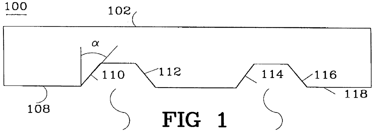
This invention solves the problem to process a micro-machined Si-mould, which forms elastomeric features or bumps with an accuracy in dimensions in the sub-micrometer range, i.e. being a perfect replication of the mould used, and easily to separate the bumps from the mould.

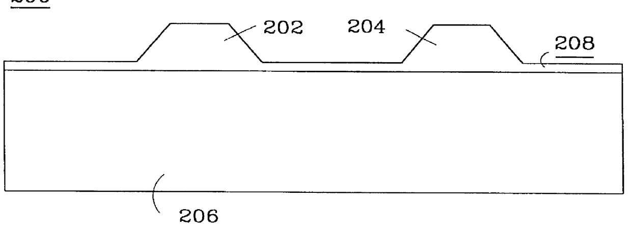
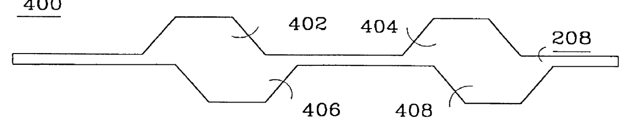
To make the elastic bumps a mould 100 is used, see FIG. 1. The prepared mould 100 is made of micro-machined Si wafer. Grooves in the mould 100 are made in the traditional way. When making the grooves 104, 106 an etch mask is used. Depending on the opening size in the etch mask, the depth and shape of the grooves 104, 106 are determined, which in turn determines the size and the shape of the bumps 202, 204, see FIG. 2. Before applying the silicone elastomer a release agent is needed because the elastomer, typically silicone elastomer, will adhere very strongly to the surface of the mould 100 during curing. The release agent can be Parylene or silane, which agent forms a release layer 118 which is conformal over the...


PUM

PropertyMeasurementUnit
Angleaaaaaaaaaa
Elastomericaaaaaaaaaa
Structureaaaaaaaaaa

Abstract

This invention relates to a manufacturing process for making elastic bumps in the micro-electronic field. It solves the problem to mould micrometer sized elastic features by means of a micro-machined mould. The method is a reproducible moulding technology to achieve elastic bumps being a perfect replication of the mould. The mould is made of one or several grooves etched in a silicon wafer. The method includes the steps of: cleaning the surface of the mould (100) from dust and other particles; depositing a release agent on the mould and the release agent, e.g. Parylene or silane, forming a conformal self-assembled layer (118) on the surface of the mould; putting on a curable elastomer, to form an elastomeric structure (208) on the mould; curing the mould and the structure; and separating the structure from the mould.

Description

The present invention relates to a manufacturing process for making bumps in the micro-electronic field, more particular to the method for moulding the elastic bump.DESCRIPTION OF RELATED ARTIn many different fields it is desirable to form small elastic features or bumps of very precise dimensions in the micrometer range. In the specific field of electronics and opto-electronics micro-miniaturisation has come very far requiring very high precision placement of parts which become very expensive unless such placement can be performed using some kind of self-alignment procedures. Also, the reduced sizes and increased speed of the electronics paths leads to increased power densities. Higher temperatures or higher temperature differences in systems pronounce thermal mismatch problems. Small elastic bumps manufactured with very high precision may be used for electric connectors and mechanical alignment of components. Elastomers, and especially silicone elastomers, are frequently used in e...

Claims


Application Information

Patent Timeline
IPC IPC(8): B29C33/64B29C33/42B29C33/62B29C33/58B29C33/38B29C33/56
CPCB29C33/3857B29C33/424B29C33/58B82Y30/00B29C33/64B82Y10/00B29C33/62
Inventor BODO, PETERHESSELBOM, HJALMAR
Owner INFINEON TECH AG
Why Eureka
Try Eureka