Programmable I/O cell with dual boundary scan

a programmable i/o cell and dual boundary scanning technology, applied in logic circuits, instruments, pulse techniques, etc., can solve the problems of high development cost, high silicon area of fpga performing any of several functions, and high development cost of redesign process (i.e., the design of hardwire replacements). , to achieve the effect of low cos

Inactive Publication Date: 2000-06-06
XILINX INC
View PDF22 Cites 42 Cited by
  • Summary
  • Abstract
  • Description
  • Claims
  • Application Information

AI Technical Summary

Benefits of technology

According to a first aspect of the invention, a hybrid HardWire device is provided that comprises a gate array core and a set of mask programmable I / O cells having I / O characteristics similar to those of the FPGA, i.e., sufficiently the same so the HardWire device can be used as a drop-in replacement for the FPGA with no redesign of the original system. A user's design originally implemented in an FPGA can be emulated in the HardWire device, which then replaces the FPGA in the same board at a lower cost.
In another embodiment, the I / O cells are programmable such that they can emulate the I / O characteristics of FPGAs from any of two or more FPGA families. The I / O cells may be mask programmable or programmable by other means such as configurable memory cells or fuses. This ability reduces the number of separate devices that must be designed, manufactured, tested, stored, and sold, and also simplifies the software required to convert designs to the new device.
According to a second aspect of the invention, a mask programmable IC is provided that includes dedicated boundary scan logic in the I / O cells. Valuable core logic resources therefore need not be consumed to implement boundary scan logic. In one embodiment, one boundary scan cell is provided per I / O cell. In another embodiment, two boundary scan cells (blocks of logic) are provided for each I / O pad, each cell alone being capable of providing the boundary scan functions associated with one FPGA I / O pad. This embodiment provides great flexibility in emulating any of several FPGAs in any of several packages. By selectively choosing which of the boundary scan cells are included in the boundary scan data chain, the order of the boundary scan chain of the emulated FPGA in any of two or more packages can be reproduced. Boundary scan behavior is therefore emulated as well as the programmed logic behavior of the FPGA. In another embodiment, more than two boundary scan cells are provided per I / O cell.

Problems solved by technology

This flexibility has its price in terms of silicon area, i.e., an FPGA performing any of several functions typically has a higher monetary cost than a device that is capable of performing only a single function.
As a result of the extensive redesign required for both Configurable Logic Blocks (CLBs) and I / O Blocks (IOBs) of multiple FPGA product families, the redesign process (i.e., the design of HardWire replacements) incurs a high development cost.
Additionally, a different HardWire product is required for each FPGA family as well as for devices of varying sizes, leading to a large number of products.
A second approach to manufacturing mask programmed replacement devices eliminates this undesirable overhead, but introduces other drawbacks.
However, a disadvantage of this method is that the I / O characteristics of the gate array are usually different from those of the FPGA, often sufficiently different to cause problems when the FPGA is removed from the system and the gate array is substituted.
An additional problem is that the gate array is incapable of emulating the configuration behavior of the FPGA unless the configuration logic is duplicated in the logic gates of the core, which results in fewer core logic gates available for the converted design.
Similarly, boundary scan is also unavailable in gate arrays unless implemented in core logic gates.
Implementing boundary scan in core logic gates uses about 72 gates per boundary scan cell, a very high cost in silicon area.

Method used


Image

  • Programmable I/O cell with dual boundary scan
  • Programmable I/O cell with dual boundary scan
  • Programmable I/O cell with dual boundary scan

Examples


second embodiment

Detailed Description of a Second Embodiment

Nine Cases are Supported

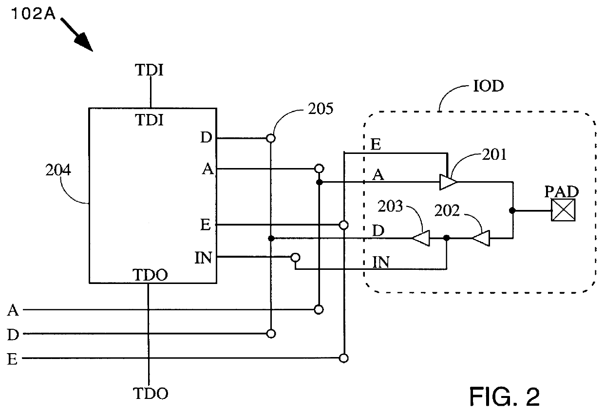
Providing two boundary scan cells per IOD makes it possible to duplicate the sequence of the boundary scan data chain in the boundary scan registers, even though a single HardWire product is used to emulate any of several FPGAs, each of which is produced in several packages. In order to support all bonding options in so many devices, the boundary scan cell must be programmable. The available options for one embodiment are as follows.

Case 1) The boundary scan logic is bypassed. This option is used, for example, when there are more boundary scan cells in the HardWire device than there are IOBs in the emulated FPGA.

Case 2) The boundary scan logic is used, and is connected to the IOD. This is the general case for a normal IOB that is bonded and used as an I / O in the emulated FPGA. Note that since Case 2 boundary scan cells are connected to the IOD, no two such cells can be placed in a single I / O cell.

Case 3) The boundary...

case 5

) The boundary scan logic is used, but is not connected to the IOD, and an additional direct path is provided from the "D" terminal of the IOD to the core. Since this boundary scan cell is not connected to the IOD, this direct path is used when emulating an FPGA input pad that does not have boundary scan, such as the PROGRAM pin of Xilinx FPGAs. The PROGRAM pin is described on page 4-47 of the Xilinx 1996 Data Book, which page is incorporated herein by reference.

case 6

) The boundary scan logic is used, but is not connected to the IOD, and two additional direct paths are provided from the "A" and "E" terminals of the IOD to the core. Since this boundary scan cell is not connected to the IOD, these direct paths are used when emulating an FPGA output pad that does not have boundary scan, such as the FPGA test data out (TDO) pin. The TDO pin is described on page 4-48 of the Xilinx 1996 Data Book, which page is incorporated herein by reference.


PUM


Abstract

A mask programmable IC is provided that includes dedicated boundary scan logic in the I / O cells. Valuable core logic resources therefore need not be consumed to implement boundary scan logic. In one embodiment, one boundary scan cell is provided per I / O cell. Another embodiment provides great flexibility in emulating any of several FPGAs in any of several packages. In this embodiment, two boundary scan cells are provided for each I / O pad, each cell alone being capable of providing the boundary scan functions associated with one I / O pad. By selectively choosing which of the boundary scan cells are included in the boundary scan data chain, the order of the boundary scan chain of the emulated FPGA in any of two or more packages can be reproduced. Boundary scan behavior is therefore emulated as well as the programmable logic behavior of the FPGA. In one embodiment, additional programmable interconnect lines traversing each boundary scan cell are provided. Theses interconnect lines can be used to programmably connect the data output of a first cell to the data input of second cell which need not be adjacent to the first.

Description

BACKGROUND OF THE INVENTION1. Field of the InventionThe invention relates to mask programmable integrated circuits (ICs). More particularly, the invention relates to mask programmable ICs manufactured to emulate Field Programmable Gate Arrays (FPGAs).2. Description of the Background ArtAn FPGA is a user-programmable device that can be programmed in the field and then re-programmed with the same or a different bitstream, to perform the same or a different function. An FPGA therefore must be capable of producing a large variety of logical behaviors. This flexibility has its price in terms of silicon area, i.e., an FPGA performing any of several functions typically has a higher monetary cost than a device that is capable of performing only a single function. Therefore, when a system including an FPGA reaches the point where it is considered unlikely to change, a manufacturer sometimes removes the FPGA from the system, and replaces the FPGA with a pin-, timing- and function-compatible r...

Claims


Application Information

Patent Timeline
Patent Type & Authority Patents(United States)
IPC IPC(8): G01R31/3185G01R31/28
CPCG01R31/318583
Inventor BAXTER, GLENN A.BUCH, KIRAN B.LAW, EDWIN S.
Owner XILINX INC
Why Eureka
Try Eureka