Method for performing quantitative measurement of DC and AC current flow in integrated circuit interconnects by the measurement of magnetic fields with a magneto optic laser probe

a magneto optic laser and interconnection technology, applied in the direction of voltage/current isolation, individual semiconductor device testing, instruments, etc., can solve the problems of insufficient semiconductor devices, inability to provide the spatial resolution necessary for probing interconnection lines, and inability to measure the current flow in semiconductor interconnection lines ("interconnect" lines)

Inactive Publication Date: 2000-07-04
INTEL CORP
View PDF13 Cites 29 Cited by
  • Summary
  • Abstract
  • Description
  • Claims
  • Application Information

AI Technical Summary

Benefits of technology

A method for measuring a magnetic field of, for example, an interconnection line, and calculating current through the line from the measured magnetic field, is provided. In the present invention, a polarized beam of radiation is passed through a material which rotates the beam in the presence of a magnetic field. The rotation is measured and used to determine the magnetic field caused by interconnection line, which in turn is used to calculate the current through the line. In the present invention, methods for calibration to eliminate the effect of variations in the material's Faraday rotation, due to such effects as temperature variations, are also described. Additionally, a method for providing a zero current reference is provided.

Problems solved by technology

However, there is currently no way to measure the current flow in semiconductor interconnection lines ("interconnect" lines) without cutting the lines or altering the lines in some way.
While Hall probes can be used to measure currents on printed circuit boards, these devices typically have a spatial resolution on the order of several thousandths of an inch (mils), which is completely inadequate for semiconductor devices.
Magneto transistors and magneto diodes have greater sensitivity than Hall probes and are smaller than Hall probes, but are still too large to provide the necessary spatial resolution for probing interconnect lines.
One problem with this method is that it requires extremely low temperatures, so that the system is difficult to implement and costly.
However, it is very difficult to separate the voltage contrast from the magnetic contrast, so that this method may not be sufficiently sensitive for measuring currents in interconnect lines.
One drawback of this method is that the frequency of the current must be approximately the same as the natural resonance frequency of the cantilever.
A further drawback of this method is the relatively low sensitivity for dc currents.

Method used


Image

  • Method for performing quantitative measurement of DC and AC current flow in integrated circuit interconnects by the measurement of magnetic fields with a magneto optic laser probe
  • Method for performing quantitative measurement of DC and AC current flow in integrated circuit interconnects by the measurement of magnetic fields with a magneto optic laser probe
  • Method for performing quantitative measurement of DC and AC current flow in integrated circuit interconnects by the measurement of magnetic fields with a magneto optic laser probe

Examples


Embodiment Construction

A laser current probe is disclosed. In the following description, numerous specific details are set forth such as specific materials, devices, equipment, schematics, testing methods, dimensions, etc. in order to provide a thorough understanding of the present invention. It will be obvious, however, to one skilled in the art that these specific details need not be employed to practice the present invention. In other instances, well known materials or methods have not been described in detail in order to avoid unnecessarily obscuring the present invention.

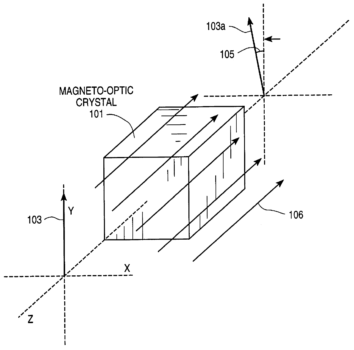
FIG. 1 illustrates the effect of magneto-optic crystal 101 on a beam of radiation in the presence of a magnetic field. As used herein, a magneto-optic material is a material that alters the properties of radiation, such as the angle of polarization, transmitted therethrough in the presence of a magnetic field. When incident electromagnetic radiation having a polarization along, for example, the y-axis as shown by vector 103 passes th...


PUM


Abstract

A laser probe for measuring a magnetic field is disclosed. A polarized laser beam is passed through a magneto-optic crystal in the presence of an unknown magnetic field. The rotation of the polarization which occurs through the magneto-optic crystal is measured in order to determine the magnitude of the magnetic field. The measured magnetic field is used to determine, for example, the current through a conductor such as an interconnect line on a semiconductor chip. A method of calibrating the magnetic field using a known magnetic from a solenoid is also disclosed. Further disclosed is a method of providing a zero-reference current by momentarily stopping the chip clock.

Description

BACKGROUND OF THE INVENTION1. Field of the InventionThe present invention relates to the measurement of electrical current through a conductor, and more specifically to the measurement of current through an interconnection line on a semiconductor device.2. Background InformationIn the semiconductor industry, it is important to characterize the internal current flow in a semiconductor device such as, for example, a microprocessor. Often, computer simulations are performed to determine the current flow under various operating conditions. With the knowledge of the current flow, and therefore the power distribution, various performance and reliability concerns can be addressed, to allow for improved performance and reliability in the functioning device.While computer simulations are useful to characterize the chip, it is desirable to measure the actual values of the internal current for a better understanding of the chip. However, there is currently no way to measure the current flow in...

Claims


Application Information

Patent Timeline
Patent Type & Authority Patents(United States)
IPC IPC(8): G01R15/24
CPCG01R15/245
Inventor RAO, VALLURI RAMANA M.
Owner INTEL CORP
Why Eureka
Try Eureka