Double poly-gate high density multi-state flat mask ROM cells

a multi-state, flat-type cell technology, applied in the direction of semiconductor devices, basic electric elements, electrical equipment, etc., can solve the problem of complex processes, and achieve the effect of high energy and improved resolution

Inactive Publication Date: 2000-07-18
ACER SEMICON MFG +1
View PDF4 Cites 13 Cited by
  • Summary
  • Abstract
  • Description
  • Claims
  • Application Information

AI Technical Summary

Problems solved by technology

Hence the processes are rather complicated or with band-to-band leakage issues.

Method used


Image

  • Double poly-gate high density multi-state flat mask ROM cells
  • Double poly-gate high density multi-state flat mask ROM cells
  • Double poly-gate high density multi-state flat mask ROM cells

Examples


Embodiment Construction

A structure of double poly gate high-density flat mask ROM cells and a method of fabricating it to achieve the purpose of multi-states on a silicon substrate are disclosed. One exemplary structure will first be described and a preferred fabricating method will then be depicted and

discussed later. The detailed mask ROM structure is best illustrated by reference to the drawings, and is described as follows.

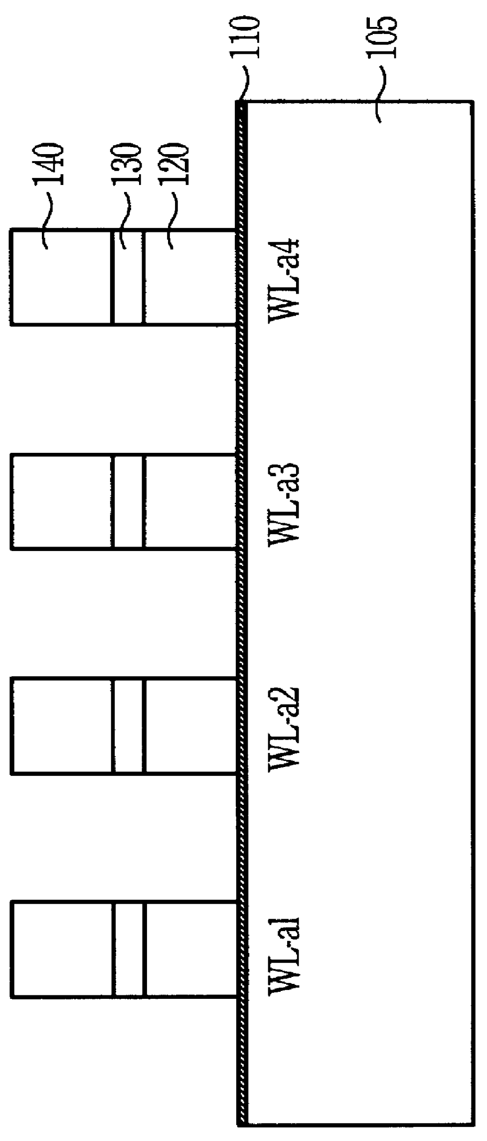
Referring to FIG. 10, a plurality of first polysilicon gates (e.g. each of first polysilicon gates comprises first nitride layer 130 / a n+ polysilicon layer 120 / a first pad oxide layer 110, and two spacers 150 ) are formed on the semiconductor substrate 105 being separated to keep a space. The first pad oxide layer 110 is formed on the semiconductor substrate 105, and a first conductive layer, a polysilicon layer 120, is formed on a portion of the first pad oxide layer 110. A first nitride layer 130 is formed on the a n+ polysilicon layer 120; and two spacers 150 is formed over remn...


PUM


Abstract

The mask ROM cell structure is described as follows: a plurality of first polysilicon gates is formed on the semiconductor substrate, being separated to keep a space. Each of first polysilicon gates comprises first nitride layer / a n+ polysilicon layer / a first pad oxide layer, and two spacers that formed over the remnant portion of the pad oxide layer, and formed, respectively, on two sidewalls of the first nitride layer 130, and the first n+ polysilicon layer. A plurality of second polysilicon gates is formed on the semiconductor substrate 105. Each of the second polysilicon gates comprises second n+doped polysilicon gate / second pad oxide layer, wherein the pad oxide layer is formed on the semiconductor substrate, and the n+doped polysilicon gate is formed on the second pad oxide layer. The first polysilicon gates separate the second polysilicon gates each.

Description

FIELD OF THE INVENTIONThe present invention relates to a semiconductor device, and more specifically, to a structure of double poly-gate high-density multi-state flat mask ROM cells.BACKGROUND OF THE INVENTIONIn recently years, the development of the portable telecommunications and laptop computers has become a major driving force in semiconductor IC's design and technology. One of most attractive semiconductor's merchandises is a very high-density non-volatile mask ROM. To achieve very high-density mask ROM, a novel semiconductor mask ROM technology incorporating a vertical cell is aiming at this objective and was proposed by Bertagnoili et al., in the reference, "B. Bertagnoili et al., `ROS: An Extremely High Density Mask ROM Technology Based On Vertical Transistor Cells`, Symp. on VLSI Tech. Dig., p, 58, 1996." The key of the technology is a cell concept based on a vertical MOS transistor in a trench which allows to use the bottom of the trench as additional -elf-aligned bit line...

Claims


Application Information

Patent Timeline
Patent Type & Authority Patents(United States)
IPC IPC(8): H01L21/8246H01L21/70H01L27/112
CPCH01L27/112H01L27/11246H01L27/1126H01L27/11266H10B20/367H10B20/383H10B20/387H10B20/00
Inventor WU, SHYE-LIN
Owner ACER SEMICON MFG
Why Eureka
Try Eureka