
Thermal monitoring system for semiconductor devices

a technology of semiconductor devices and monitoring systems, applied in the field of measuring temperatures, can solve the problems of increasing not being able to monitor the operating temperature of the semiconductor device, and not being able to solve the problem of increasing the heat generated by the increase in packaging density,

Inactive Publication Date: 2000-07-25
IBM CORP
View PDF7 Cites 51 Cited by
  • Summary
  • Abstract
  • Description
  • Claims
  • Application Information

AI Technical Summary

Problems solved by technology

This continued integration of more electronic circuitry into semiconductor devices is not without undesirable consequences.
One of these undesirable consequences or side-effects is the increase in heat generated due to the increase in packaging density.
Although these work well in many applications, the operating temperature of the semiconductor device is not monitored and therefore not known during the operation of the semiconductor device.
Measuring the operating temperature of a semiconductor device is difficult in applications where the top of the device is covered by a heat sink, a fan, or both.
For example, the bottom surface the semiconductor device may have indentations, and other irregularities that do not provide a direct contact to the sensor.

Method used


Image

  • Thermal monitoring system for semiconductor devices
  • Thermal monitoring system for semiconductor devices
  • Thermal monitoring system for semiconductor devices

Examples


Embodiment Construction

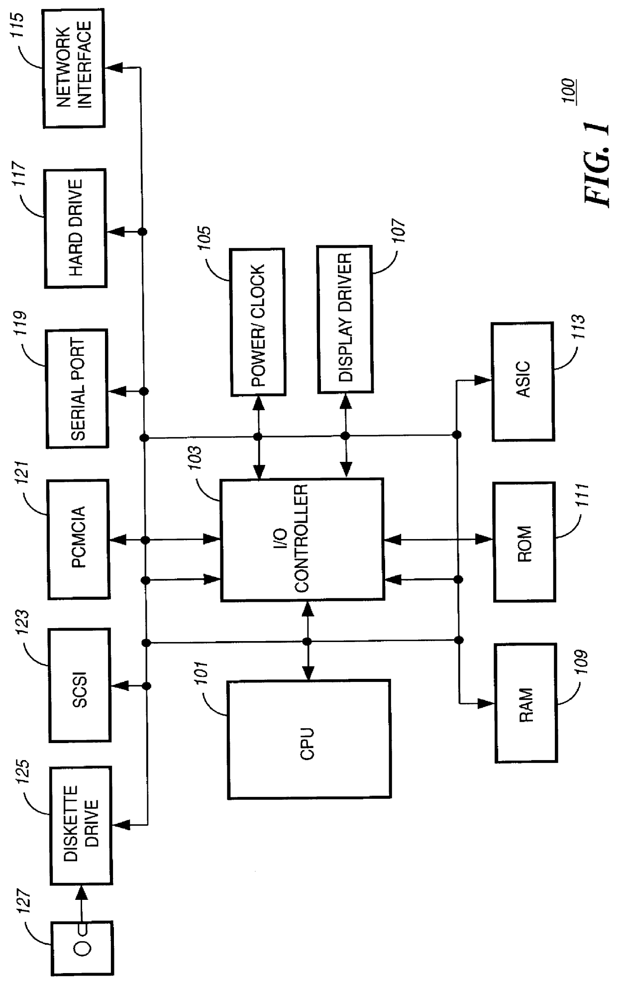
Referring to FIG. 1, there is shown a block diagram of the major electrical components of an information processing device 100 in accordance with this invention. The electrical components include: a central processing unit (CPU) 101, an Input / Output (I / O) Controller 103, a system power and clock source 105; display driver 107; RAM 109; ROM 111; ASIC (application specific integrated circuit) 113 and a hard disk drive 117. These are representative components of a computer. The operation of a computer comprising these elements is well understood. Network interface 115 provides connection to a computer network such as Ethernet, TCP / IP or other popular protocol network interfaces. Optional components for interfacing to external peripherals include: a Small Computer Systems Interface (SCSI) port 123 for attaching peripherals; a PCMCIA slot 121; and serial port 119. An optional diskette drive 125 is shown for loading or saving code to removable diskettes 127. The system 100 may be implemen...


PUM


Abstract

A method for monitoring the operating temperature of a semiconductor device. The method comprising the steps of: placing a thermal coupling material between the bottom of the semiconductor device and the top of a printed circuit board for inserting the device thereinto; inserting a sensor so to be at least partially covered by the thermal coupling material; and measuring the temperature from the sensor within a predetermined time interval. In accordance with another aspect of the invention, an apparatus is described to carry out the above process.

Description

Not applicable1. Field of the InventionThis invention relates generally to the field of thermal monitoring and more particularly to the field of measuring temperatures during semiconductor operations.2. Description of the Related ArtAs semiconductor integration continues to make advances, the packaging densities of semiconductor devices continues to increase. The number of transistors on semiconductor devices has doubled every couple of years. This continued integration of more electronic circuitry into semiconductor devices is not without undesirable consequences.One of these undesirable consequences or side-effects is the increase in heat generated due to the increase in packaging density. Several solutions have been employed for removing heat from semiconductor devices. These solutions include heat sinks, cooling fans, and in some cases, liquid cooling. Today many commercially available semiconductor devices, especially microprocessors, such as those used in personal computers fr...

Claims


Application Information

Patent Timeline
IPC IPC(8): G01K7/42
CPCG01K7/42
Inventor STILL, STEPHEN EUGENEGARCIA, RAYHONEYCUTT, KENDALL ANTHONYTOUT, JR., JAMES J.
Owner IBM CORP
Learn More