Tapered rib waveguide
a technology of rib waveguides and tapered ribs, which is applied in the direction of optical waveguide light guides, optical light guides, instruments, etc., can solve the problems of relatively complex and/or difficult fabrication
- Summary
- Abstract
- Description
- Claims
- Application Information
AI Technical Summary
Benefits of technology
Problems solved by technology
Method used
Image
Examples
Embodiment Construction
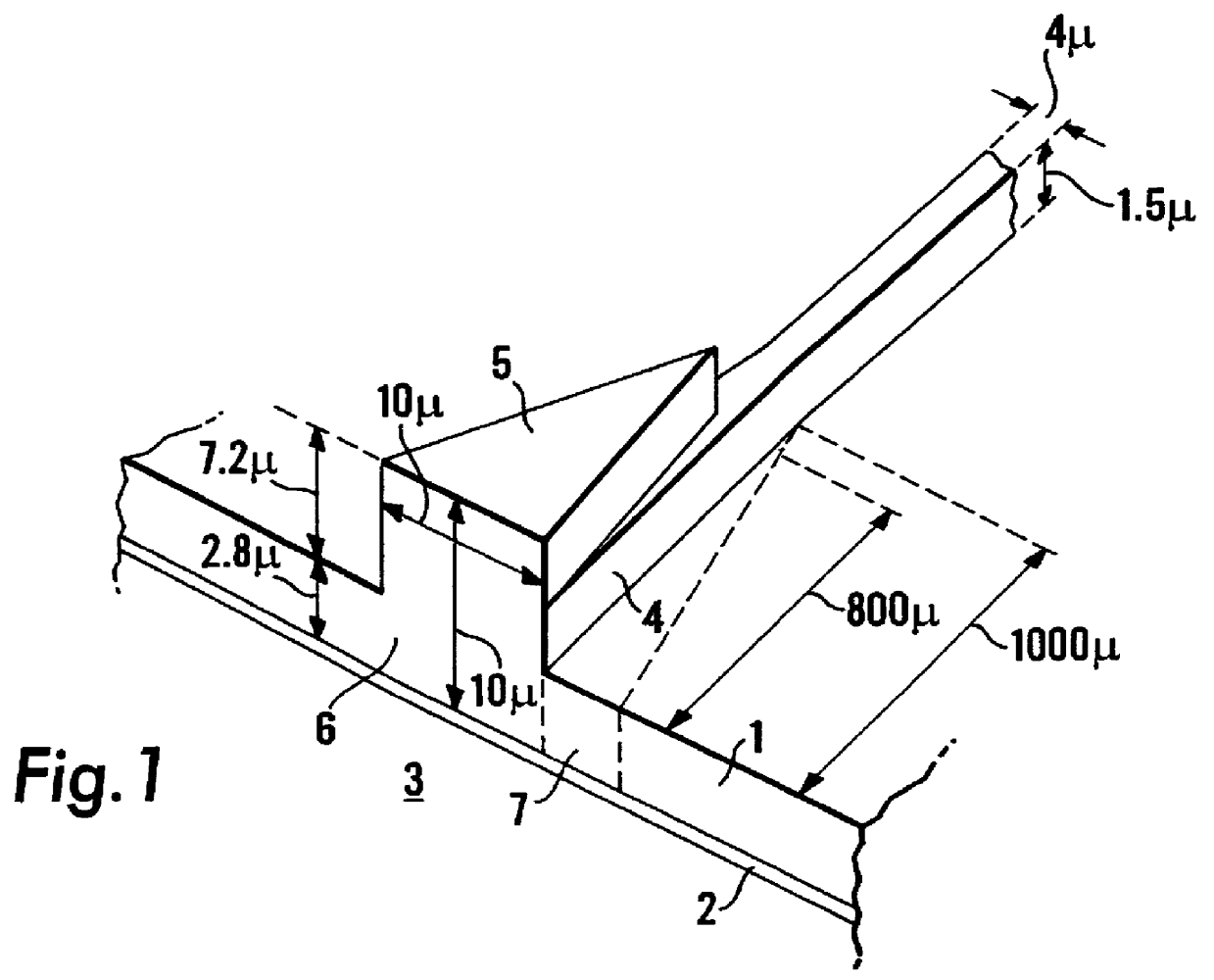
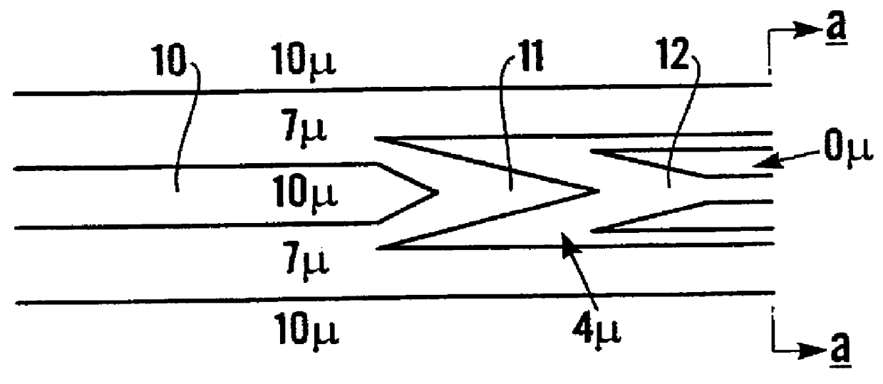
The drawing shows a tapered rib waveguide tapering from a large multi-mode waveguide about 10 microns.times.10 microns to a smaller single-mode waveguide about 4.3 microns.times.4 microns.
The illustrated waveguides are in the form of ribs formed on the upper surface of a silicon layer, e.g. of a silicon-on-insulator chip. The silicon-on-insulator chip is preferably manufactured from conventional wafers such as those used in Very Large Scale Integration (VSLI) electronic circuits. The paper "Reduced defect density in silicon-on-insulator structures formed by oxygen implantation in two steps" by J. Morgail et al, Appl. Phys. Lett, 54, p 526, 1989 describes the manufacture of suitable wafers. Methods of manufacturing rib waveguides on a silicon-on-insulator chip are described in the paper "Low loss single mode optical waveguides with large cross-section in silicon-on-insulator" by J. Schmidtchen et al, Electronic Letters, 27, p 1486, 1991.
The drawing shows the rib waveguides formed in ...
PUM
 Abstract
Description
Claims
Application Information


