Display device

a display device and display screen technology, applied in the field of display devices, can solve the problems of reducing the effective area of a pixel and darkening the screen

Inactive Publication Date: 2000-09-05
SEMICON ENERGY LAB CO LTD
View PDF31 Cites 101 Cited by
  • Summary
  • Abstract
  • Description
  • Claims
  • Application Information

AI Technical Summary

Problems solved by technology

However, the black matrix has a demerit that it reduces an effective area of a pixel (this rate will be referred to as an aperture ratio) and darkens the screen.

Method used


Image

  • Display device
  • Display device
  • Display device

Examples


first embodiment

[First Embodiment]

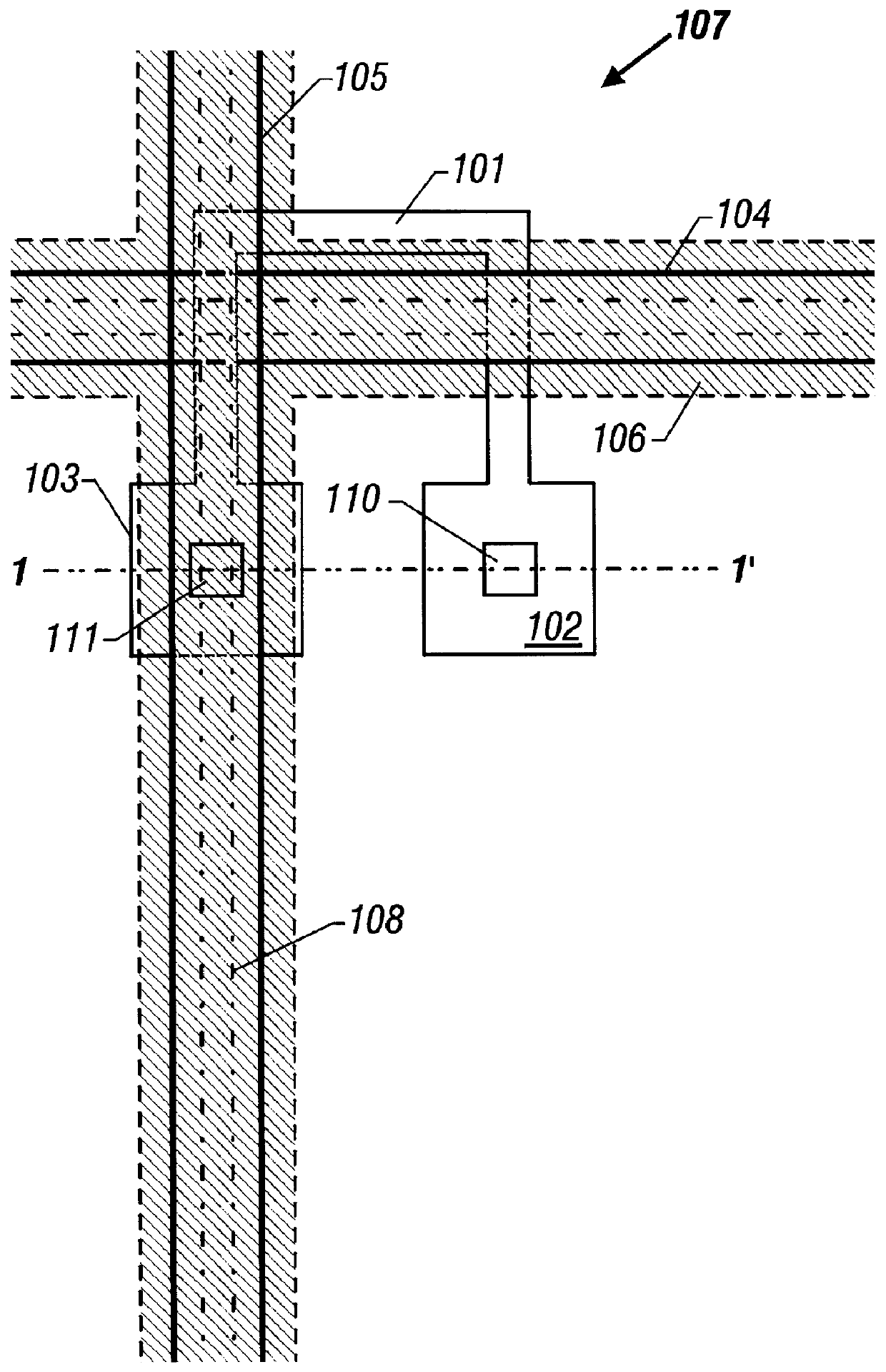
FIGS. 1 through 3 show the structure of the present embodiment. FIGS. 1 through 3 are enlarged plan views showing part of one pixel of an active matrix type liquid crystal display.

FIGS. 1 through 3 show the same part. The structure thereof will be explained with reference to FIG. 1 at first. In FIG. 1, a pattern 101 constitutes an active layer of a thin film transistor. The active layer 101 is made of a crystal silicon film.

A reference numeral 102 which is part of the active layer 101 is a region called as a drain region. A reference numeral 103 is a region called as a source region. These regions are N-type in case of N-channel type and are P-type in case of P-channel type.

A pattern 104 is a gate line. Regions in the active layer 101 at the part where the gate line 104 overlaps with the active layer 101 are channel regions. Regions where the gate line 104 overlaps with the active layer 101 function as gate electrodes.

A source line 105 contacts with the source regi...

second embodiment

[Second Embodiment]

The present embodiment relates to a structure modified from that shown in the first embodiment. The source line and the gate line have been overlapped with the pixel electrode and the overlap regions have been caused to function as the black matrix in the structure shown in the first embodiment. The structure shown in the first embodiment has been useful in increasing the aperture ratio to the maximum. However, it is necessary to increase the area of the black matrix depending on a requested image quality or a displaying method.

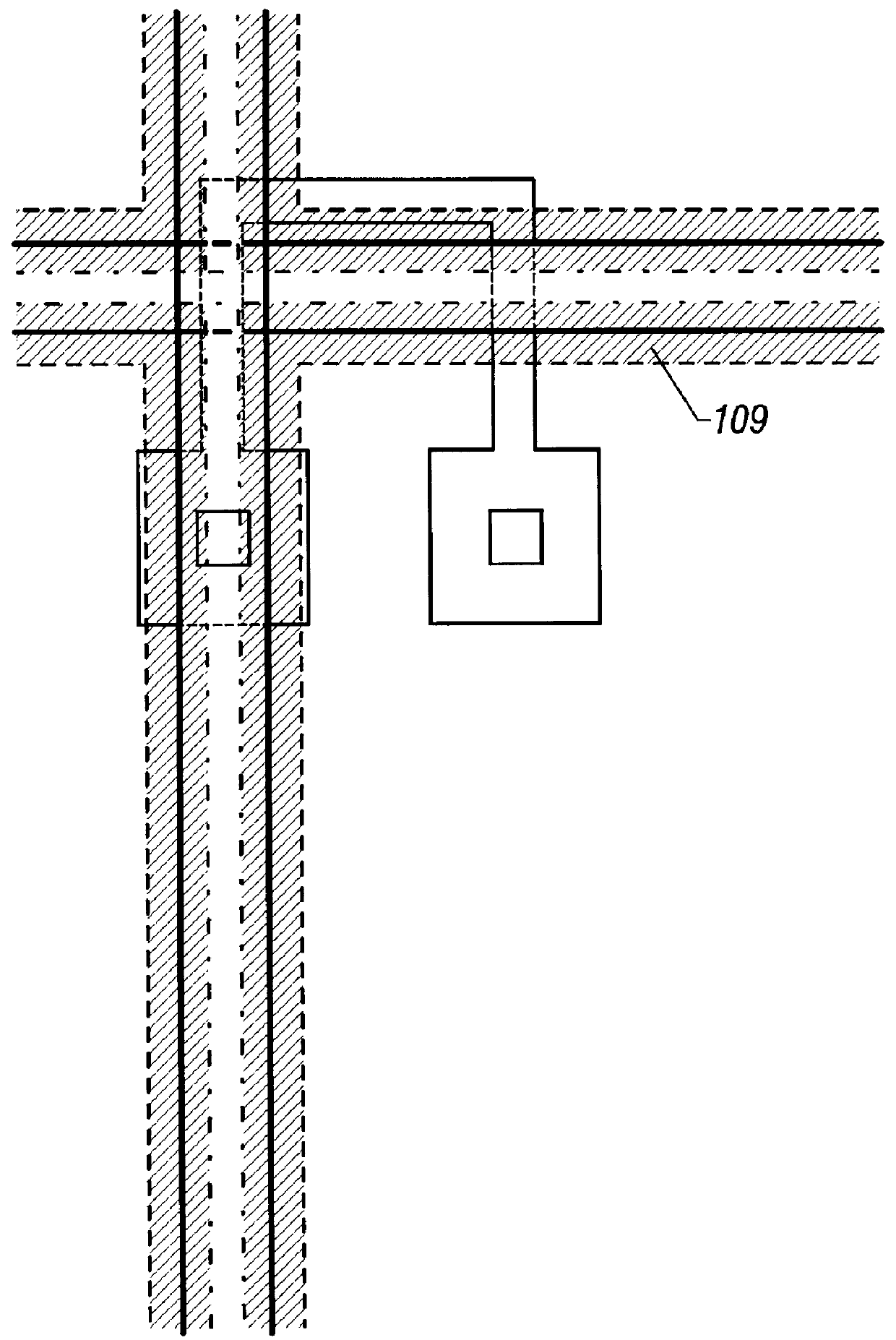
The present embodiment relates to a structure which can be utilized in such a case. FIG. 11 shows a section of a pixel part according to the present embodiment. FIG. 11 corresponds to FIG. 10 and the same reference numerals with those in FIG. 10 denote the same components in FIG. 11.

In the present embodiment, part of a film 1102 which is made of a titanium film or chromium film (or an adequate metallic film) and which constitutes the black ...


PUM

PropertyMeasurementUnit
thicknessaaaaaaaaaa
thicknessaaaaaaaaaa
thicknessaaaaaaaaaa

Abstract

The present invention provides an active matrix type display device having a high aperture ratio and a required auxiliary capacitor. A source line and a gate line are overlapped with part of a pixel electrode. This overlapped region functions to be a black matrix. Further, an electrode pattern made of the same material as the pixel electrode is disposed to form the auxiliary capacitor by utilizing the pixel electrode. It allows a required value of auxiliary capacitor to be obtained without dropping the aperture ratio. Also, it allows the electrode pattern to function as a electrically shielding film for suppressing the cross-talk between the source and gate lines and the pixel electrode.

Description

The invention disclosed in the present specification relates to a structure of a liquid crystal display or a fabrication method thereof.DESCRIPTION OF RELATED ARTThere has been known a flat panel display typified by a liquid crystal display. In a transmission type liquid crystal display having a mode of optically modulating light which has passed through a liquid crystal panel by the liquid crystal panel, light shielding means called a black matrix is required in order to clearly define a profile of pixels. In concrete, it is necessary to cover the peripheral portion of a pixel electrode by a light shielding frame. Such a black matrix plays an important role in displaying fine motion pictures in particular.However, the black matrix has a demerit that it reduces an effective area of a pixel (this rate will be referred to as an aperture ratio) and darkens the screen.It is being tried to utilize the flat panel display in low power consumption type portable equipments such as a portable...

Claims


Application Information

Patent Timeline
Patent Type & Authority Patents(United States)
IPC IPC(8): G02F1/13G02F1/1362G02F1/136G02F1/1368G02F1/1343
CPCG02F1/136213G02F1/136227G02F1/136209B66C1/04B66C9/08B66C13/06
Inventor ZHANG, HONGYONGTERAMOTO, SATOSHI
Owner SEMICON ENERGY LAB CO LTD
Why Eureka
Try Eureka