Anisotropic conductive sheet and printed circuit board

Inactive Publication Date: 2000-09-19
SHINKO ELECTRIC IND CO LTD
View PDF12 Cites 83 Cited by
  • Summary
  • Abstract
  • Description
  • Claims
  • Application Information

AI Technical Summary

Problems solved by technology

However, there are problems in that a production process becomes longer to increase a production cost because the electric connections between the respective layers are made through via-ho

Method used


Image

  • Anisotropic conductive sheet and printed circuit board
  • Anisotropic conductive sheet and printed circuit board
  • Anisotropic conductive sheet and printed circuit board

Examples


Embodiment Construction

The present invention will be described in detail below with reference to the preferred embodiments illustrated in the attached drawings.

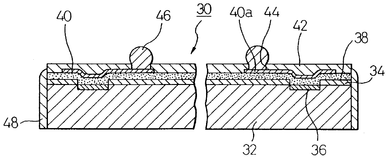
FIG. 1 is a side sectional view of a semiconductor device 30 using an anisotropic conductive sheet with a conductive layer described later, according to the present invention.

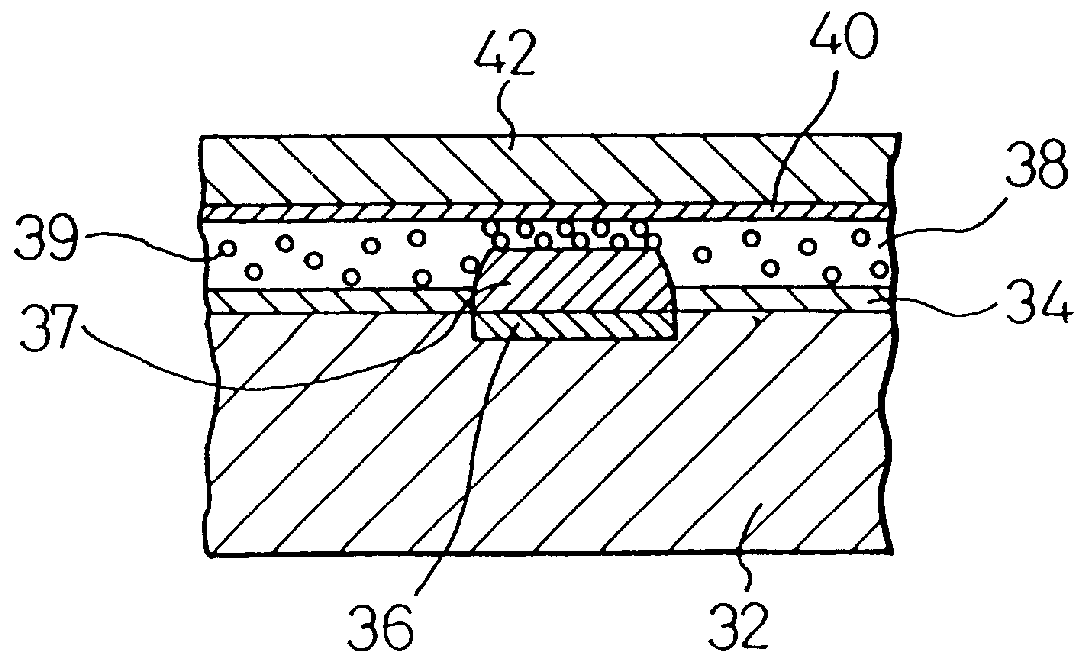
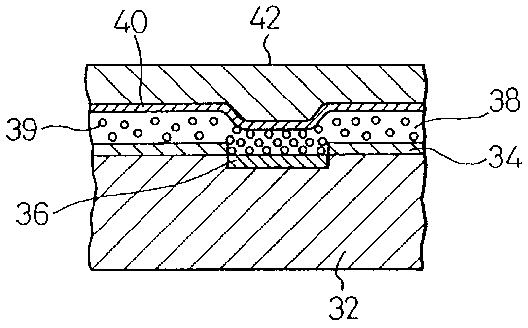
Reference numerals 32 denotes a semiconductor chip; 34, a passivation film made of SiO.sub.2 or others; and 36, an Al pad (pad section) built in the semiconductor chip 32. The passivation film 34 is not formed in an area where the Al pad 36 exists, so that the Al pad 36 is exposed. A number of Al pads 36 are formed in a desired pattern on the semiconductor chip 32.

Reference numeral 38 denotes an anisotropic conductive sheet formed while covering the passivation film 34. The anisotropic conductive sheet 38 is formed of a resin containing a conductive filler 39 (FIG. 2) such as a metallic powder, and, by the application of pressure, becomes conductive in the pressed direction du...


PUM


Abstract

An anisotropic conductive sheet material includes a resin and conductive fillers, such as metallic particles, added in the resin. A conductive layer is formed on one of the surfaces of the anisotropic conductive sheet material. A circuit board includes a substrate having first and second surfaces and a circuit pattern being formed on the first surface of the substrate, an anisotropic conductive sheet having first and second surfaces, a circuit pattern being formed on the first surface thereof. The second surface of the anisotropic conductive sheet is adhered to the first surface of the substrate in such a manner that the circuit patterns are electrically connected to each other by means of the anisotropic conductive sheet. An electrically insulative layer formed on the first surface of the anisotropic conductive sheet to cover the circuit pattern thereof, except that external connecting portions thereof are exposed.

Description

1. Field of the InventionThe present invention relates to an anisotropic conductive sheet with a conductive layer and a printed circuit board using the same. The present invention also relates to a semiconductor device using such an anisotropic conductive sheet.2. Description of the Related ArtA multilayer type printed circuit board consisting of a plurality of resin substrates, each carrying circuit patterns on its surface, has been known in the art.According to such a multilayer type printed circuit board, it is possible to form highly integrated circuit patterns because the degree of freedom increases for wiring circuit patterns.However, there are problems in that a production process becomes longer to increase a production cost because the electric connections between the respective layers are made through via-holes having a film formed by an electroless plating on the inner wall thereof, and a thickness of the resultant product becomes larger because a plurality of resin substr...

Claims


Application Information

Patent Timeline
IPC IPC(8): H01L21/02H01L21/60H01L23/52H01L23/532H01L23/498H01L23/48H05K3/46H05K3/40H05K1/03H05K3/32
CPCH01L23/49816H01L23/49827H01L23/5328H01L24/28H01L24/31H01L24/83H05K3/4617H01L24/12H01L2224/13022H01L2224/8319H01L2224/838H01L2924/01005H01L2924/01013H01L2924/01029H01L2924/01033H01L2924/01046H01L2924/01047H01L2924/0105H01L2924/01078H01L2924/01079H01L2924/01082H01L2924/0781H01L2924/14H01L2924/19041H01L2924/19043H05K1/0373H05K3/323H05K3/4084H05K3/4647H05K2201/0215H01L2224/13016H01L2224/2919H01L2224/83851H01L2924/01006H01L2924/014H01L2924/0665H01L2224/81903H01L2924/0132H01L2224/2929H01L2924/00014H01L2924/1517H01L2924/1579H01L2224/29111H01L2224/293H01L2224/13111H01L2224/29339H01L2224/29355H01L2224/05124H01L2224/05147H01L2224/05624H01L2224/05647H01L2224/0615H01L2224/02377H01L21/60
Inventor AKAGAWA, MASATOSHI
Owner SHINKO ELECTRIC IND CO LTD
Why Eureka
Try Eureka