Low voltage class AB amplifier with gain boosting

a low-voltage class ab amplifier and gain booster technology, which is applied in the direction of dc-amplifiers with dc-coupled stages, amplifiers with semiconductor devices/discharge tubes, and differential amplifiers, etc., can solve the problems of increasing the complexity of the circuit, affecting the performance of the amplifier, and reducing the power supply voltage requirements. , to achieve the effect of increasing the gain and reducing the voltage requirements

Inactive Publication Date: 2000-10-03
NAT SEMICON CORP
View PDF9 Cites 25 Cited by
  • Summary
  • Abstract
  • Description
  • Claims
  • Application Information

AI Technical Summary

Problems solved by technology

However, as the power supply voltage decreases, it becomes more difficult to maintain sufficiently high gain without increasing the complexity of the circuitry.
However, this can significantly increase the complexity of the circuit.
This is particularly undesirable in the case of integrated circuits which have already become, and continue to be, increasingly complex already.
A major disadvantage of this feed forward type of circuit, however, is the fact that it has a relatively high minimum operating voltage requirement (V.sub.DD(min) -V.sub.SS) of approximately 2.7 volts.
Accordingly, this minimum voltage requirement makes this circuit unsuitable for operation with a 1.8 volt power supply voltage.
However, a significant disadvantage of this feedback type of circuit is the limited DC gain due to the limited number (two) of gain stages.

Method used


Image

  • Low voltage class AB amplifier with gain boosting
  • Low voltage class AB amplifier with gain boosting
  • Low voltage class AB amplifier with gain boosting

Examples


Embodiment Construction

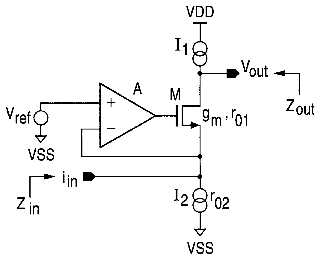
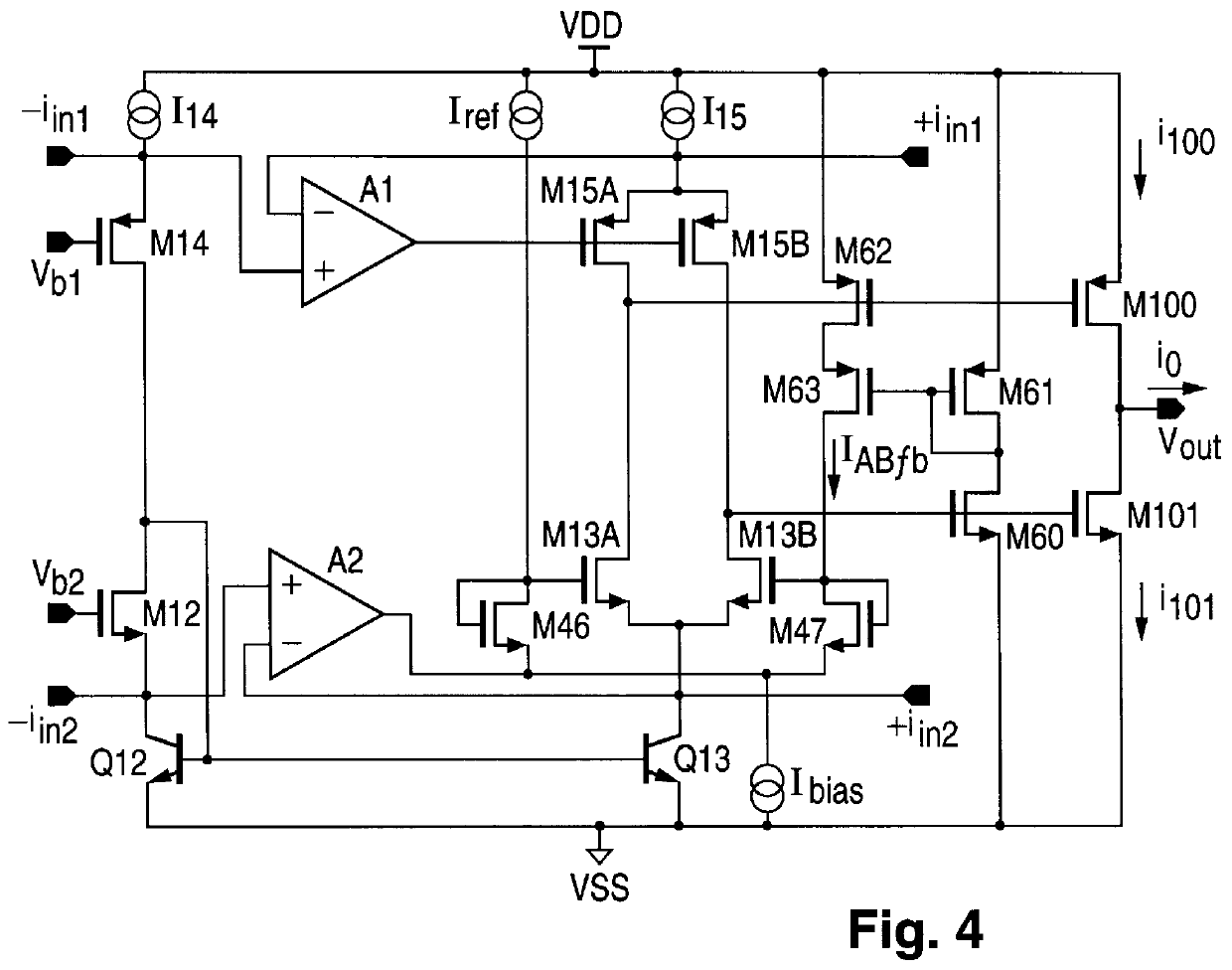
Referring to FIGS. 4 and 5, a low voltage amplifier with gain boosting and reduced power supply voltage requirements in accordance with one embodiment of the present invention uses gain boosting to increase the gain of the circuit of FIG. 3. Tithe two additional amplifiers A1, A2 provide gain boosting to cascode MOS transistors M15A, M15B, M13A and M13B and improve output impedance (as discussed above) by dynamically controlling the biasing at the gate terminals of transistors M15A, M15B, M13A and M13B.

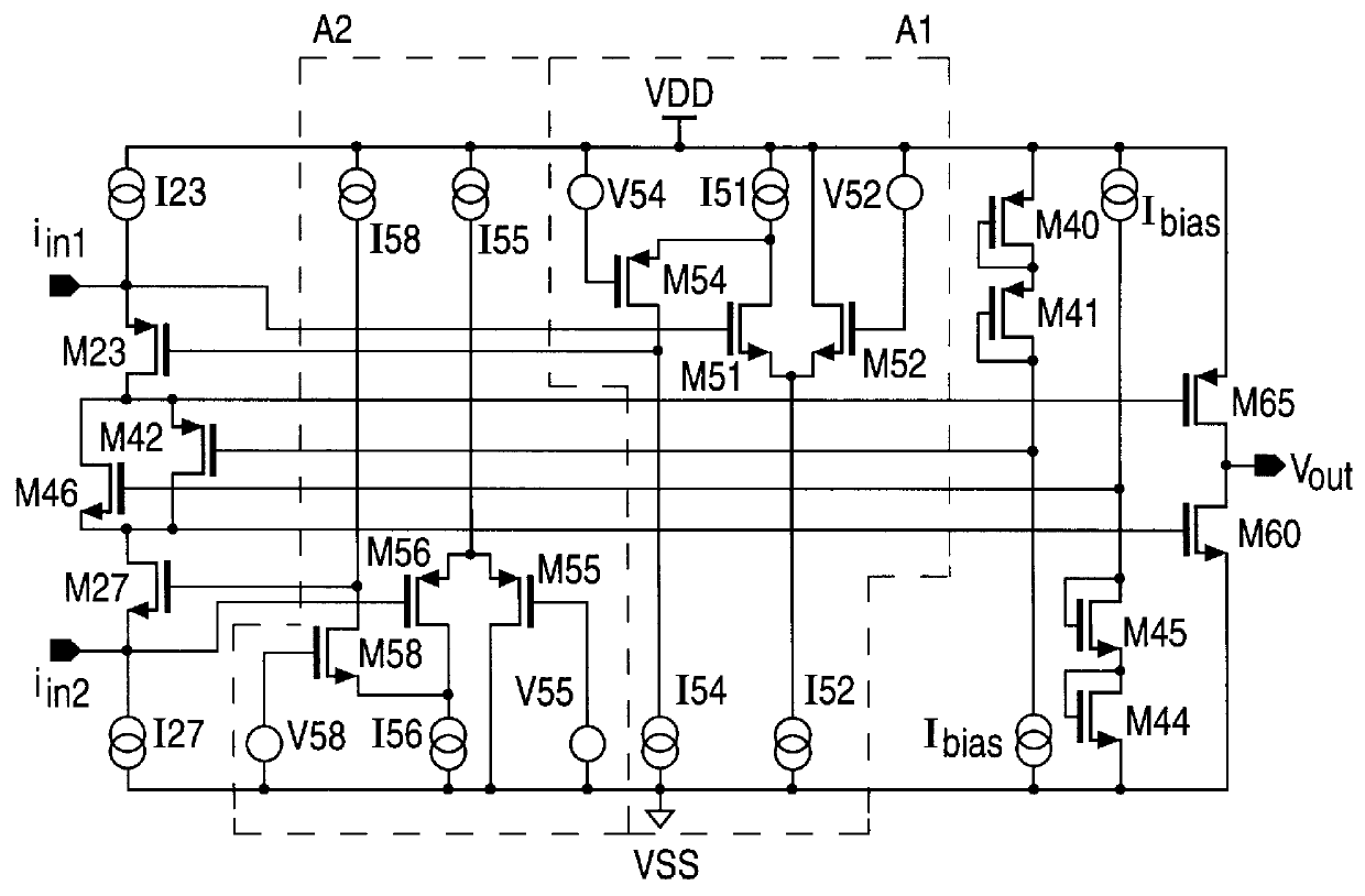
As shown in more detail in FIG. 5, amplifier A1 is implemented using a cascode differential-to-single-ended amplifier (transistors M1, M2 and M41). The high output impedance of this amplifier A1 matches the high impedance load of the gate terminals of transistors M15A and M15B. Amplifier A2, however, requires a low impedance output since it is driving a low impedance load of diode connected transistors M46 and M47. Therefore, amplifier A2 is implemented by a cascode differential-to-si...


PUM


Abstract

A low voltage amplifier with gain boosting and a reduced power supply voltage requirement. A cascode amplifier circuit, biased with the power supply voltage, amplifies a pair of related, differential input signals based upon a pair of gain boost control signals and in accordance therewith provides a pair of gain boosted signals which correspond to the input signals. A gain boost control circuit, also biased with the power supply voltage, uses the differential input signals to generate the gain boost control signals. A class AB amplifier circuit, also biased with the power supply voltage, amplifies the gain boosted signals and in accordance therewith provides a class AB output signal which corresponds to the original input signals. The cascode amplifier circuit, gain boost control circuit and class AB amplifier circuit together operate with a minimum power supply voltage which equals a sum of one active transistor input bias potential and two active transistor output bias potentials

Description

BACKGROUND OF THE INVENTION1. Field of the InventionThe present invention relates to class AB amplifiers, and in particular, to low voltage class AB amplifiers with gain boosting and reduced power supply voltage requirements.2. Description of the Related ArtAs the demand for portable, battery operated devices has increased and transistor geometries continue to shrink, the use of low voltage circuits (i.e., circuits which operate at reduced power supply voltages, such as 2.5 and 1.8 volts) continue to increase. However, as the power supply voltage decreases, it becomes more difficult to maintain sufficiently high gain without increasing the complexity of the circuitry. For example, in low voltage circuits, high DC gain is generally achieved by cascading several gain stages. However, this can significantly increase the complexity of the circuit. This is particularly undesirable in the case of integrated circuits which have already become, and continue to be, increasingly complex alrea...

Claims


Application Information

Patent Timeline
Patent Type & Authority Patents(United States)
IPC IPC(8): H03F3/30
CPCH03F3/303H03F3/3032H03F2203/45574
Inventor ESCHAUZIER, RUDY G. H.ZAKAI, REHAN A.
Owner NAT SEMICON CORP
Why Eureka
Try Eureka