

Substrate processing apparatus
a processing apparatus and substrate technology, applied in the direction of coatings, metallic material coating processes, chemical vapor deposition coatings, etc., can solve the problems of increased materials cost and deteriorated mass production efficiency, and achieve excellent mass production efficiency, reduce materials cost, and facilitate manufacturing
- Summary
- Abstract
- Description
- Claims
- Application Information
AI Technical Summary
Benefits of technology
Problems solved by technology
Method used
Image

Examples
first example
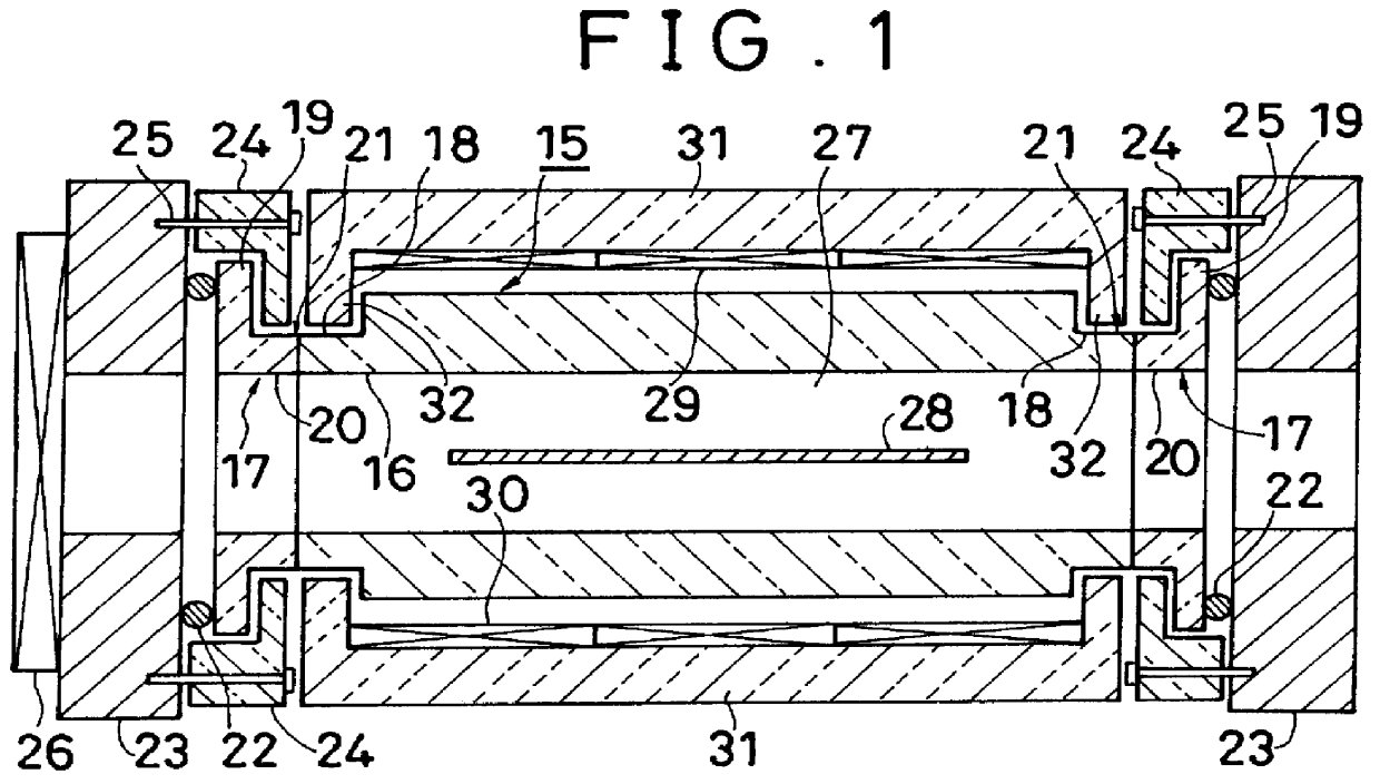
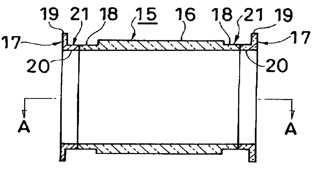
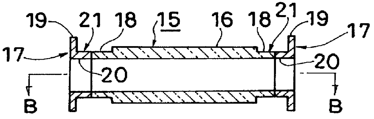
In the case of the reaction furnace used for film formation process of a wafer having a diameter of 8 inches, degree of vacuum in the reaction chamber 27 is kept at 0.01 to 10 torr. If outside dimension of the reaction chamber 27 is such that width 320 mm.times.height 80 mm.times.axial length 540 mm, plate thickness of the cylindrical body 16 excluding both the opposite ends 18 is set to 20 mm, plate thickness of
the recess 21 is set to 10 mm, and width of the recess 21 is set to 70 mm.
second example
In the case of the reaction furnace used for film formation process of a wafer having a diameter of 12 inches, degree of vacuum in the reaction chamber 27 is kept at 0.01 to 10 torr. If outside dimension of the reaction chamber 27 is such that width 440 mm.times.height 100 mm.times.axial length 690 mm, plate thickness of the cylindrical body 16 excluding both the opposite ends 18 is set to 20 to 35 mm, preferably 30 to 35 mm, plate thickness of the recess 21 is set to 10 mm, and width of the recess 21 is set to 70 mm.
It is needless to say that plate thickness of the cylindrical body, plate thickness of the both ends, and width of the recess may be changed in accordance with a shape of the cylindrical body and degree of vacuum.
According to the present invention, as described above, since the recess is provided in the outer face of the reaction container and the wall thickness is made thin, weld-joining is easy, it is unnecessary to carve quartz to integrally form the flange, the cost...
PUM
| Property | Measurement | Unit |
|---|---|---|
| diameter | aaaaa | aaaaa |
| thickness | aaaaa | aaaaa |
| axial length | aaaaa | aaaaa |
Abstract
Description
Claims
Application Information