Method of exposing thermoresist

a technology of thermoresist and insulating layer, which is applied in the field of exposing thermoresist, can solve the problems of not being able to have a practical true thermoresist, not being able to shield from ambient temperature, and being lower resolution

Inactive Publication Date: 2000-10-24
CREO PRODS
View PDF28 Cites 16 Cited by
  • Summary
  • Abstract
  • Description
  • Claims
  • Application Information

AI Technical Summary

Problems solved by technology

An even larger problem is caused when trying to image high resolution features: the point spread function of the optical system causes a "spreading" of light from each feature.
This causes light from on feature to overlap with adjacent features and lower the resolution.
It is not possible to have a practical true thermoresist which follows the reciprocity law.
While it is possible to shield a photoresist from ambient light it is not possible to shield from ambient temperature.
Therefore a practical thermoresist cannot obey the reciprocity law.
The limiting factor in both these patents is the leakage light from the light valves used.
Even if the light valves were ideal, the limited optical resolution of the imaging lens creates a probl

Method used


Image

  • Method of exposing thermoresist
  • Method of exposing thermoresist
  • Method of exposing thermoresist

Examples


Embodiment Construction

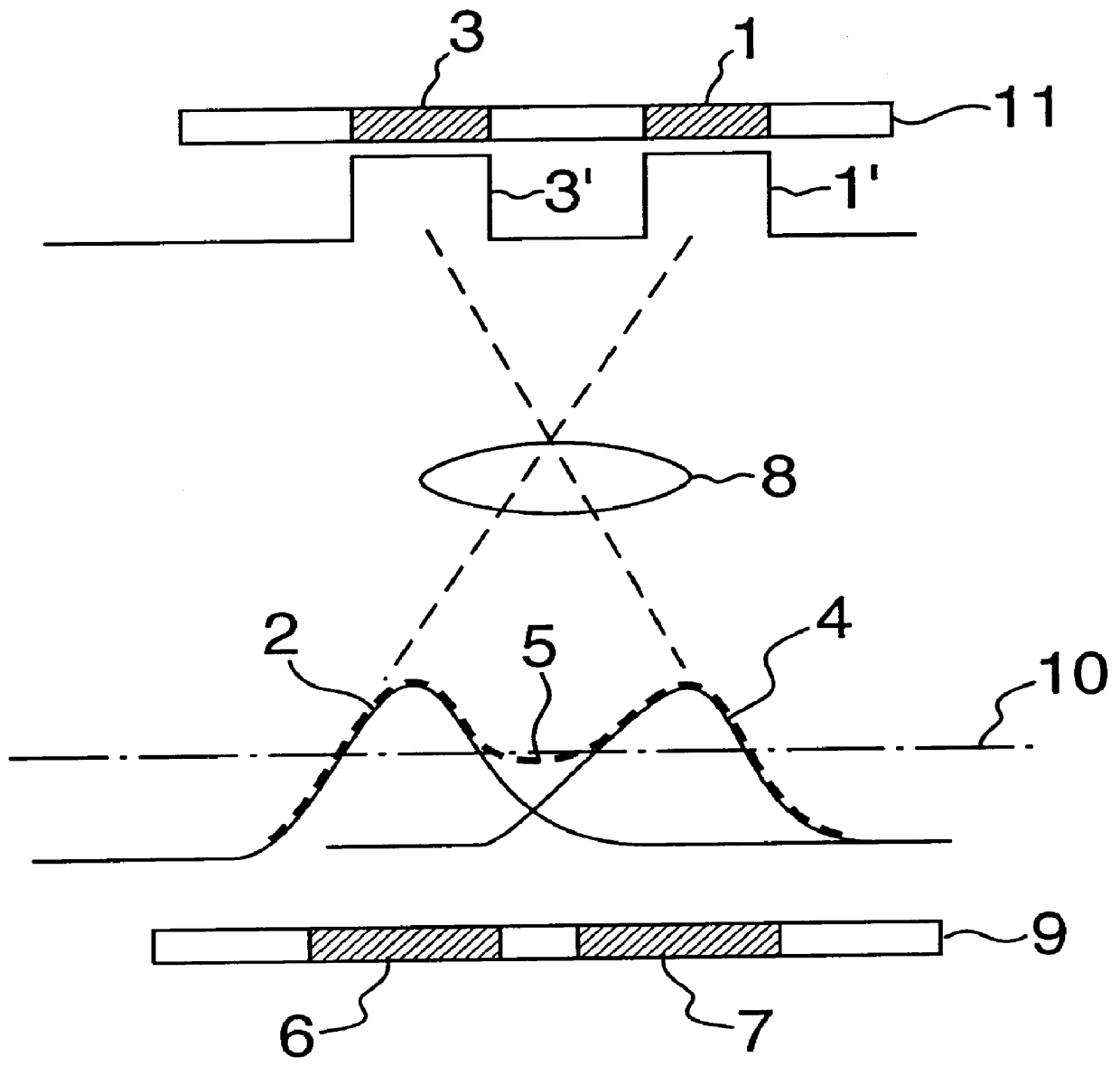
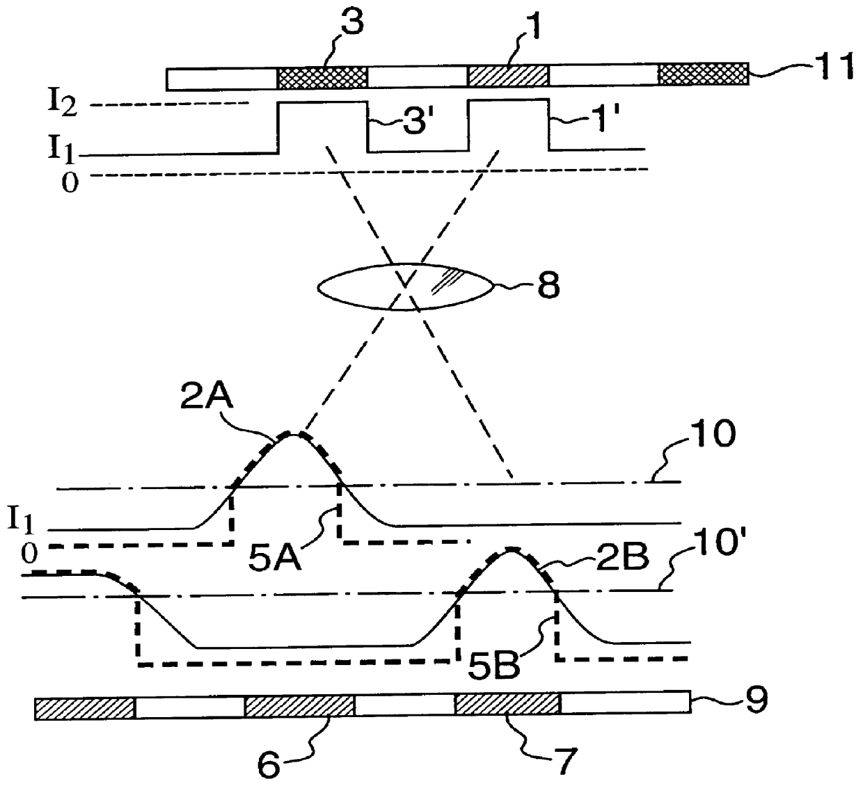
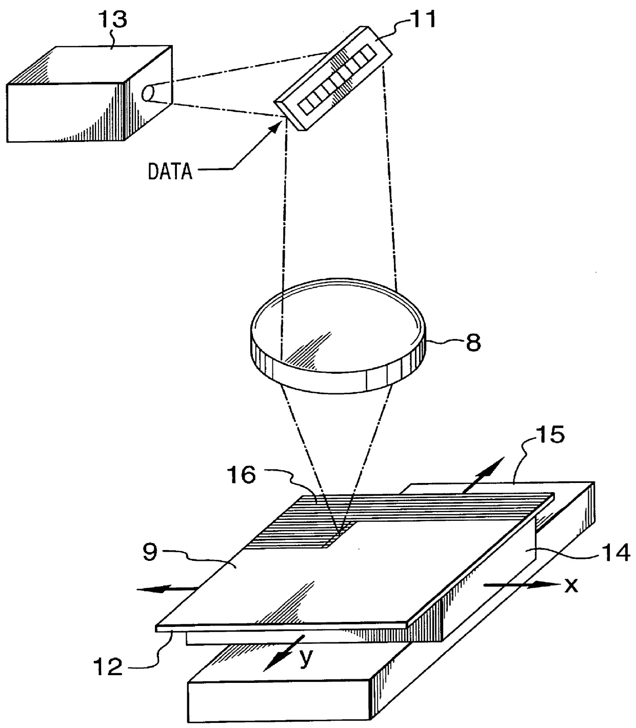
copper-clad inner layer of a printed circuit board was coated with Difine 4LF thermal resist by dip coating. A pattern of one pixel on / one pixel off was imaged on a Creo Trendsetter operating at 2400 dpi, as well as a 2 pixel on / 2 pixel off pattern. Each pixel is about 10.6 microns (1 / 2400"). After imaging the resist was developed according to the data sheet, using standard developer. The Trendsetter is available from Creo Products Inc. (Vancouver, Canada) and the Difine 4LF thermoresist is available from Creo Ltd. (Lod, Israel). The Trendsetter uses a light valve. The light leakage was set at 5%. Even at this relatively high light leakage, the 2 pixel on / 2 off pattern was imaged sharply in a single exposure, far exceeding results achieved with photoresists. The 1 on / 1 off pattern was broken up. When the 1 on / 1 off pattern was imaged in 2 passes, each pass consisting of 1 on / 3 off and passes staggered by 2 pixels (i.e.: odd lines imaged in one pass and even lines imaged in second pa...


PUM


Abstract

Low contrast optics, including low contrast linear light valves, can be used to create high resolution patterns by using thermoresist instead of photoresist and by using multiple exposures of the same area, preferably exposing different features of the pattern in each exposure. When using thermoresist, the stray light from imaging the individual features does not add up, as the stray heat it creates will dissipate between exposures. The method is particularly useful for imaging thermoresists using UV light for manufacturing of integrated circuits.

Description

The invention relates to imaging of etch resistant layers also known as "resists", in order to fabricate high resolution patterns by etching or deposition. In particular, the invention relates to the manufacturing of integrated circuits, flat panel displays and printed circuit boards.BACKGROUND ON THE INVENTIONThe processes for fabricating high resolution patterns, mainly on planar objects, by selective etching or deposition has been well known for centuries. In general, the layer to be shaped or patterned is covered by a protective layer known as a "resist". The desired shapes are created in the protective layer, usually via photo-imaging. The exposed (or unexposed, if the resist is negative working) part of the image is removed, normally by using a liquid developer to expose the layer underneath. The exposed layer can now be etched through the openings in the resist layer, which protects the covered area from the etching process. Etching can be by wet chemicals or by dry plasma (a...

Claims


Application Information

Patent Timeline
IPC IPC(8): G03F7/20H05K3/00
CPCG03F7/2022G03F7/70291G03F7/70358G03F7/70466G03F7/70383Y10S430/146H05K3/0082
Inventor GELBART, DANIEL
Owner CREO PRODS
Why Eureka
Try Eureka