

Programmable SRAM and DRAM cache interface with preset access priorities
- Summary
- Abstract
- Description
- Claims
- Application Information
AI Technical Summary
Benefits of technology
Problems solved by technology
Method used
Image

Examples
Embodiment Construction
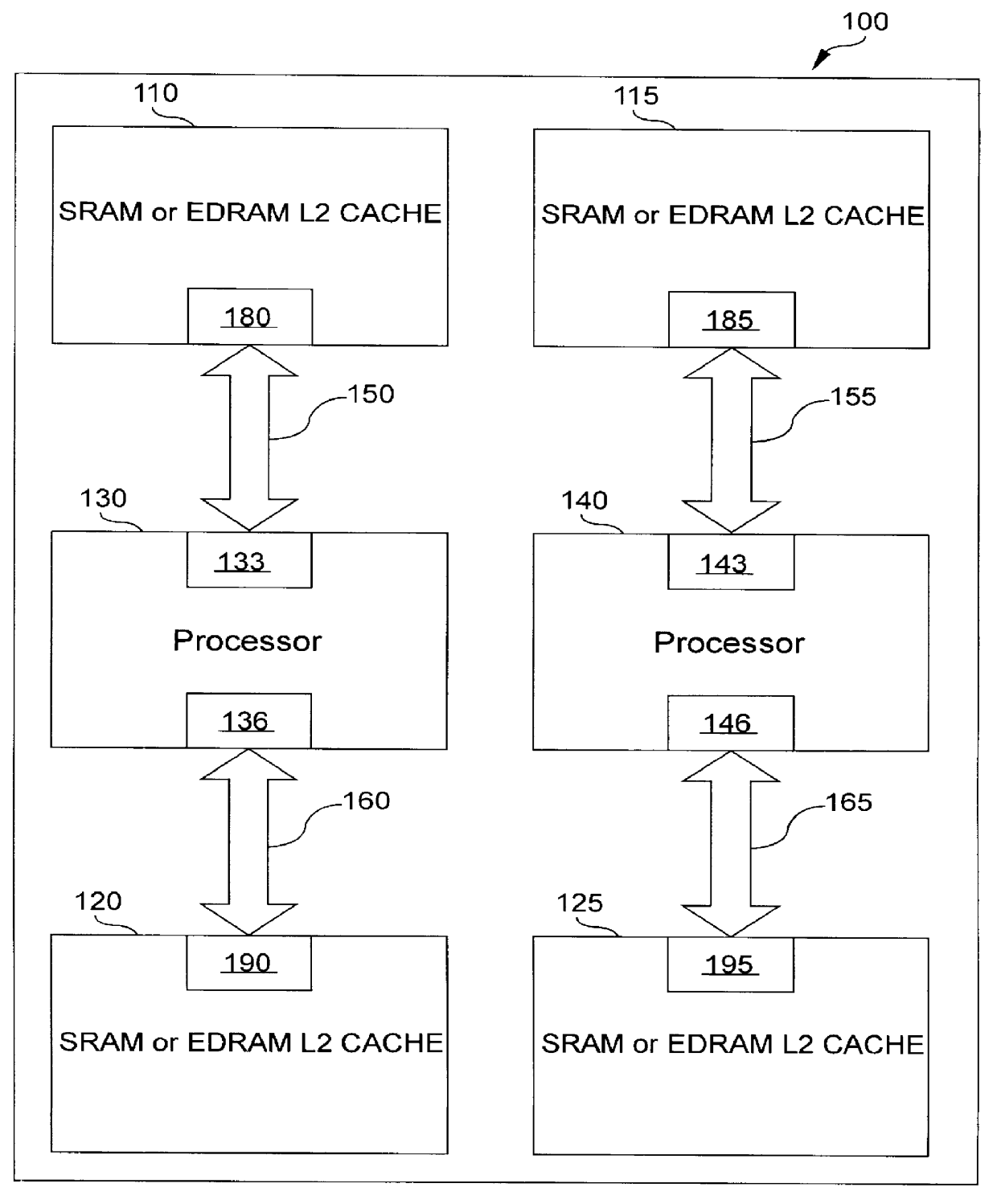
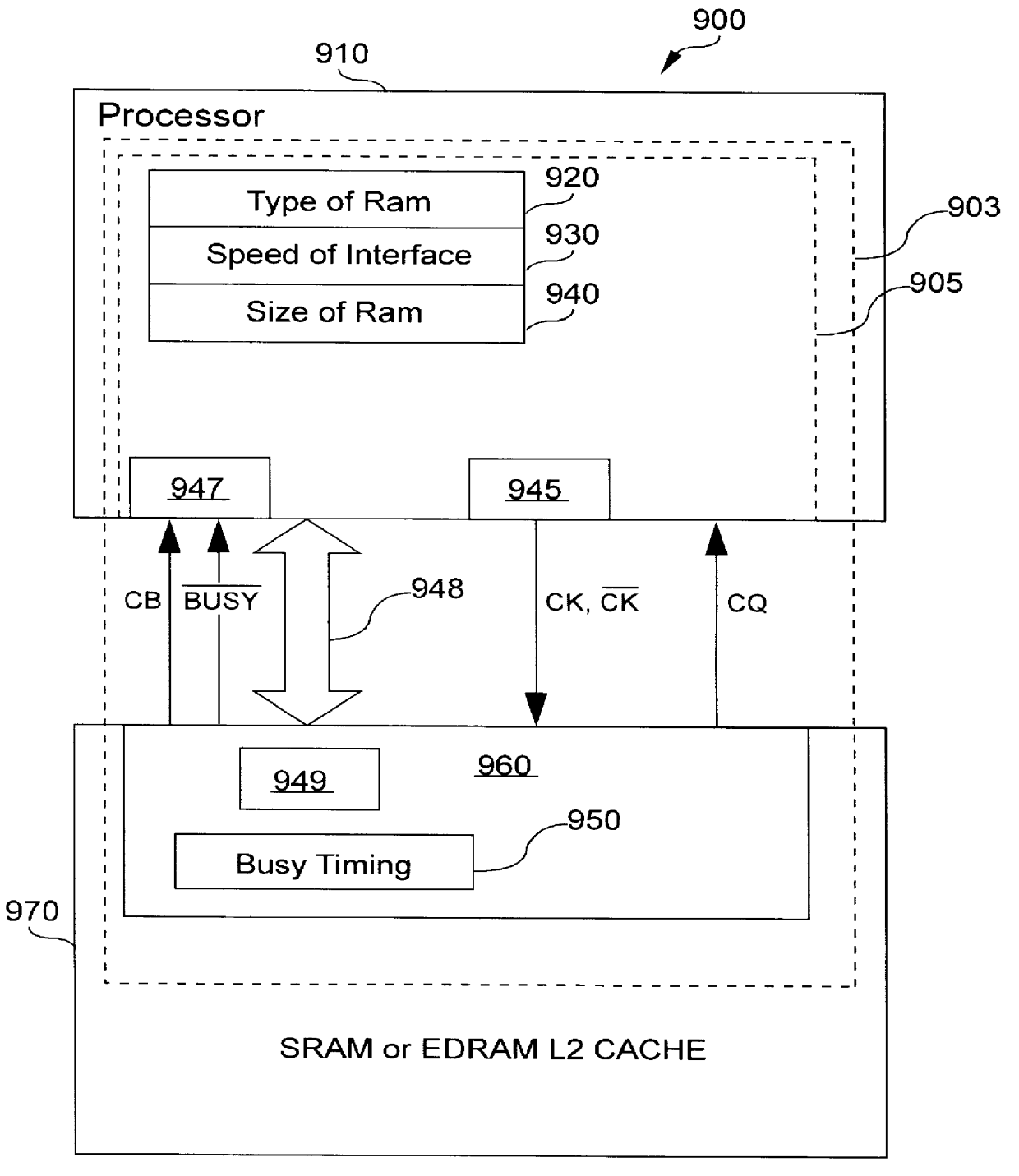
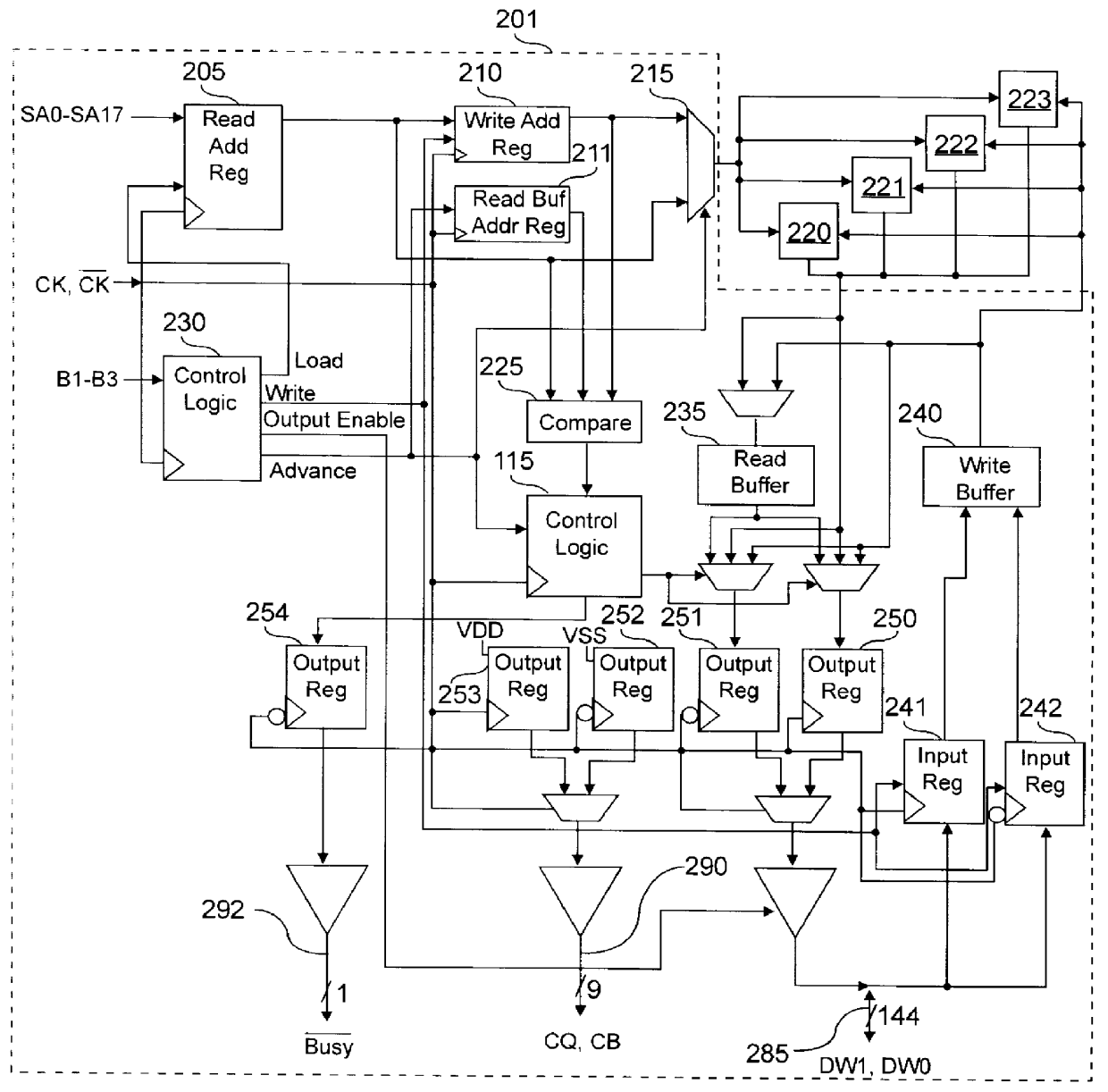
A cache interface that supports both Static Random Access Memory (SRAM) and Dynamic Random Access Memory (DRAM) is disclosed. The cache interface preferably comprises two portions, one portion on the processor (preferably as part of the L2 cache controller) and one portion on the cache. The processor portion of the cache interface is programmable to support a DRAM or an SRAM L2 (or higher) cache, multiple different cache speeds, and different cache sizes. Thus, the processor portion of the cache interface should not need to change for the processor to access a wide variety of different size, speed, and types of caches. The cache portion of the cache interface is, however, preferably allowed to change to best support different cache RAM (DRAM or SRAM).
It is important to note that the current invention works with caches and cache arrays that are comprised of RAM that does have to be refreshed (DRAM) and RAM that does not have to be refreshed (SRAM). While only DRAM will be discussed, ...
PUM
 Abstract
Description
Claims
Application Information