Optical module and lead frame for optical module

a technology of optical modules and lead frames, which is applied in the direction of semiconductor devices, semiconductor/solid-state device details, radiation control devices, etc., can solve the problems of difficult to secure an area for mounting circuit elements, the number of outer lead pins cannot be reduced, and the packing density of the semiconductor assembly cannot improv

Inactive Publication Date: 2000-12-05
SUMITOMO ELECTRIC IND LTD
View PDF6 Cites 24 Cited by
  • Summary
  • Abstract
  • Description
  • Claims
  • Application Information

AI Technical Summary

Benefits of technology

Thus, drawing the wiring leads in predetermined directions can provide an optical module lead frame which is suitable for high-density packaging and appropriate for connecting with an optical waveguide.

Problems solved by technology

Additional outer lead pins are required for connecting the respective semiconductor elements mounted on the different lead frames to each other, whereby the number of the outer lead pins cannot be reduced even when this configuration is employed.
It cannot improve the packing density of the semiconductor assembly.
As the distance between the light-emitting element and the light-receiving element becomes shorter, the circuit element portion must be made smaller depending on this distance, whereby it is hard to secure an area for mounting the circuit elements.
When a main amplifier, a clock data reproducing circuit, and the like, in addition to the preamplifier, are mounted to the circuit element mounting portion, the mounting area for such additional circuit devices cannot be secured.

Method used


Image

  • Optical module and lead frame for optical module
  • Optical module and lead frame for optical module
  • Optical module and lead frame for optical module

Examples


first embodiment

(First Embodiment)

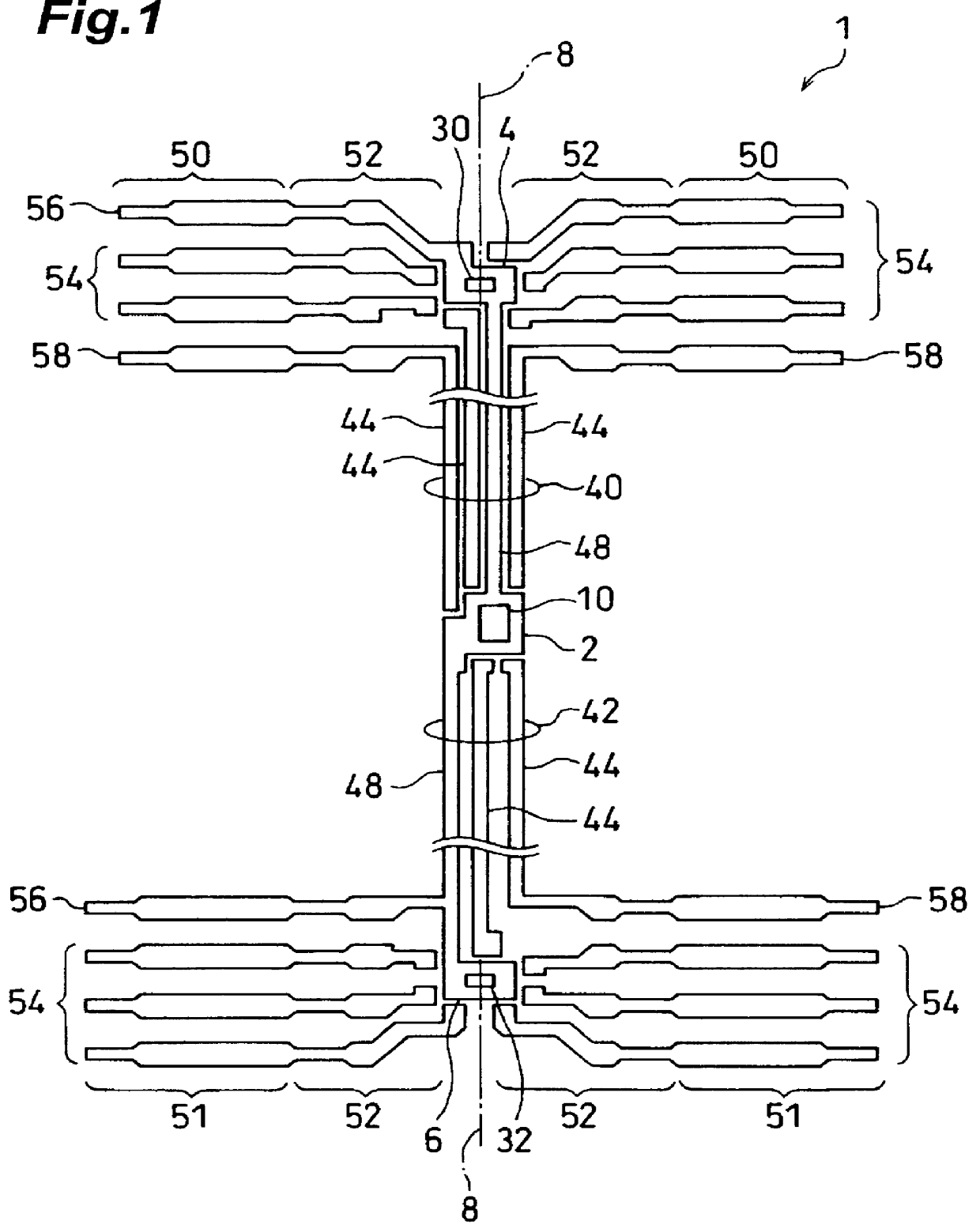
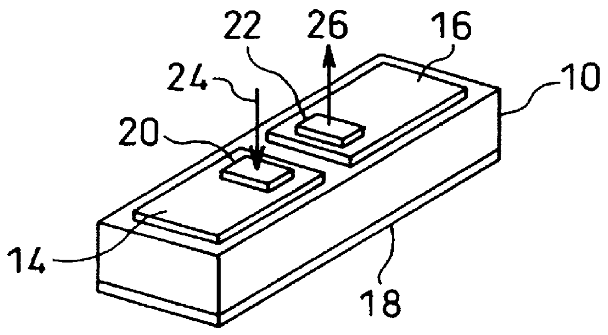
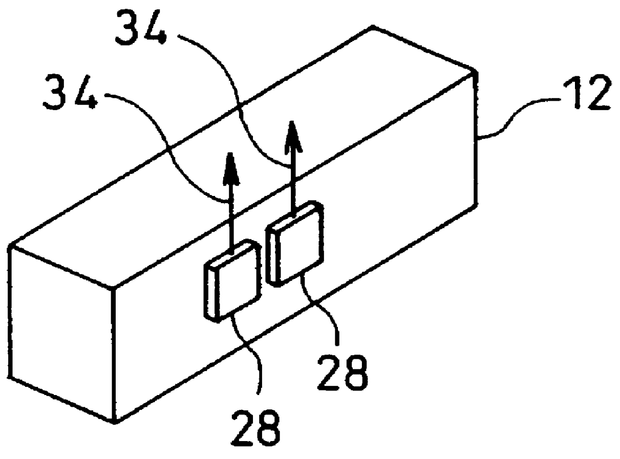
FIG. 1 is a plan view of a main portion of the lead frame in accordance with the first embodiment. Referring to FIG. 1, the lead frame 1 comprises a planar first die pad 2, made of electric conductive material, located at the center thereof; and two planar second die pads 4, 6, each made of electric conductive material, disposed on both sides of the first die pad 2. The three die pads 2, 4, 6 are included in the same plane and are arranged along a single line. One main surface of the lead frame 1 includes the mounting surface of the first die pad 2 and the mounting surfaces of the second die pads 4, 6. A plurality of optical devices are mounted on the mounting surface of the first die pad 2, whereas semiconductor circuit devices (hereinafter referred to as circuit devices) 30, 32 are mounted on the mounting surfaces of the second die pads 4, 6. The circuit devices 30, 32 are electrically connected to the optical devices, thereby processing electric signals associat...

second embodiment

(Second Embodiment)

FIG. 7 is a plan view of a major portion of the optical module lead frame in accordance with the second embodiment. Referring to FIG. 7, this lead frame 101 has a basic configuration similar to that of the first embodiment. Namely, the lead frame 101 comprises a planar first die pad 102, made of a electric conductive material, located at the center thereof; and two planar second die pads 104, 106, each made of a conductive material, disposed on both sides of the first die pad 102. The three die pads 102, 104, 106 are contained within the same plane and are arranged on a single line. The mounting surface of the first die pad 102 and the mounting surfaces of the second die pads 104, 106 coincide with one main surf ace of the lead frame 1. Further, the lead frame 101 has connection lead groups 140, 142, and wiring leads 154, 156, 158. The first and second connection lead groups 140, 142 have a plurality of conducting connection leads 144, 148, provided for electrical...

third embodiment

(Third Embodiment)

FIG. 10 is a plan view of a major portion of the optical module lead frame 201 in accordance with the embodiment. The lead frame 201 shown in FIG. 10 will not be explained in detail because it has substantially the same configuration as that of the lead frame 101 in the second embodiment except for the configuration concerning the directions in which wiring leads 254, 256, 258 are drawn. Individual parts of the lead frame 101 in the second embodiment and their corresponding parts of the lead frame 201 in the third embodiment are referred to with reference numerals whose lower two digits are common in FIGS. 7 and 10, except for the optical devices 10 and the circuit devices 30, 32, and the like.

FIGS. 11A and 12A are perspective views of optical module in which the light-receiving device 20, light-emitting device 22, circuit devices 30, 32, and the like are mounted on their corresponding die pads 202, 204, 206 and encapsulated with resin. Referring to FIGS. 11A and 1...


PUM


Abstract

PCT No. PCT/JP98/04310 Sec. 371 Date Jul. 9, 1999 Sec. 102(e) Date Jul. 9, 1999 PCT Filed Sep. 25, 1998 PCT Pub. No. WO99/16133 PCT Pub. Date Apr. 1, 1999An optical module, including a plurality of optical devices and a plurality of circuit devices, which is suitable for a smaller size and a higher density, and a lead frame for the optical module are provided. The optical module comprises optical devices, circuit devices 30, 32 electrically connected to the optical devices; a lead frame mounting these devices on the same main surface; and a first encapsulating resin body 66, transparent to light processed by the optical devices, for encapsulating the optical devices. The lead frame has a single first die pad for mounting a plurality of optical devices; a plurality of second die pads 4, 6 each for mounting a circuit device; connection lead groups 40, 42, whose number is the same as that of the second die pads, having a plurality of connection leads 44, 48 for electrically connecting the optical devices mounted on the first die pad to the circuit devices mounted on the second die pads 4, 6; and wiring leads 50, 51 arranged so as to face the respective side faces of the second die pads 4, 6. In the optical module, the optical devices are connected to the wiring leads 50, 51 by way of the connection leads 44, 48.

Description

The present invention relates to an optical module and a lead frame for the optical module; and, in particular, to an optical module mounting a plurality of optical devices and a plurality of semiconductor circuit devices on the same lead frame, and the lead frame for the optical module.Attempts have conventionally been made to attain the higher packing density of parts using a lead frame. As an example of such attempts, there is a technique disclosed in Japanese Patent Application Laid-Open No.1-257361. FIG. 15 is a sectional view of the semiconductor assembly disclosed in the above-mentioned publication. Referring to FIG. 15, semiconductor elements 404, 404' are mounted on the surfaces of two lead frames 401, 401', respectively. Electrode pads on the individual semiconductor elements 404, 404' are connected to their corresponding inner leads by bonding wires 403, 403', respectively. Then, with their rear faces faced to each other, the two lead frames 401, 401' are overlaid on each...

Claims


Application Information

Patent Timeline
Patent Type & Authority Patents(United States)
IPC IPC(8): H01L25/16H01L23/52H01L31/02H01L33/54H01L33/56H01L23/48H01L33/62
CPCH01L25/167H01L2224/48247H01L2224/48091H01L2924/00014
Inventor FUKUOKA, TAKASHI
Owner SUMITOMO ELECTRIC IND LTD
Why Eureka
Try Eureka