Method of manufacturing semiconductor device comprising high voltage regions and floating gates

a manufacturing method and high-voltage region technology, applied in the direction of semiconductor devices, electrical devices, transistors, etc., can solve the problems of lowering the performance efficiency of logic devices, the method of manufacturing semiconductor devices, and the inability to obtain high junction breakdown voltage in the high-voltage applied region of high-voltage devices

Inactive Publication Date: 2000-12-12
HYUNDAI MICRO ELECTRONICS CO LTD
View PDF5 Cites 47 Cited by
  • Summary
  • Abstract
  • Description
  • Claims
  • Application Information

AI Technical Summary

Problems solved by technology

The conventional method of manufacturing a semiconductor device has a number of problems.
For example, in the manufacturing method of a system on a chip as described, the high-voltage device and logic device have the same source / drain regions, and a short-channel device with a high impurity concentration cannot be made in the logic device thereby lowering the performance efficiency of the logic device.
Further, in the formation of a short-channel device in the logic device, a high junction breakdown voltage cannot be obtained in the high-voltage applied region of the high-voltage device due to the semiconductor substrate of high concentration and the shallow source / drain region.
Thus, the performance efficiency of the high-voltage device is reduced.

Method used


Image

  • Method of manufacturing semiconductor device comprising high voltage regions and floating gates
  • Method of manufacturing semiconductor device comprising high voltage regions and floating gates
  • Method of manufacturing semiconductor device comprising high voltage regions and floating gates

Examples


Embodiment Construction

Reference will now be made in detail to the preferred embodiments of the present invention, examples of which are illustrated in the accompanying drawings.

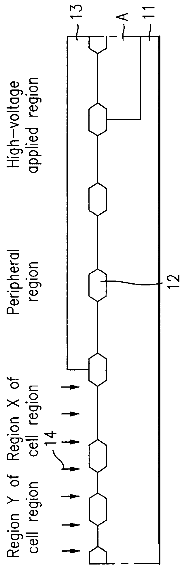
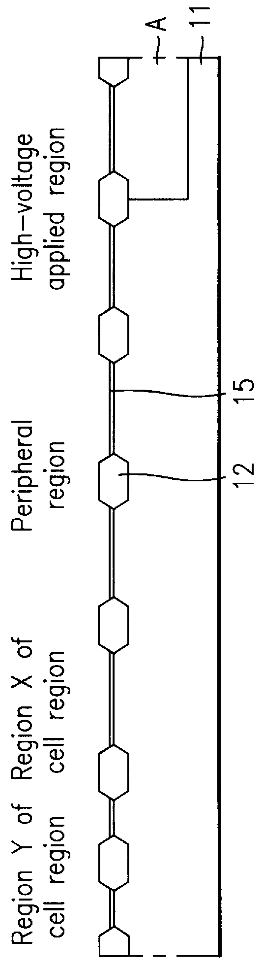
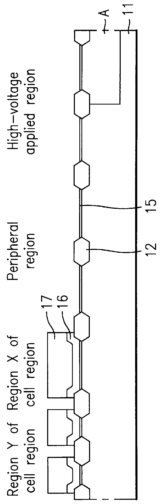
FIGS. 2A to 2J illustrate a method of manufacturing a semiconductor device in accordance with the present invention.

According to the method of manufacturing a semiconductor device, as shown in FIG. 2A, regions Y and X of a cell region, a peripheral region, a high-voltage applied region, and a separation region are defined in a p-type semiconductor substrate 31. The cell region and the high-voltage applied region correspond to a high-voltage device while the peripheral region corresponds to a logic device. An n-well B is formed in a portion of the high-voltage applied region where a PMOS will be formed, and an oxidation process is carried out on substrate 31 of the separation region to form a plurality of field oxide films 32.

A first photoresist film 33 is deposited of the substrate 31 including field oxide films 32. The first phot...


PUM


Abstract

A method of manufacturing a semiconductor device includes the steps of preparing a substrate having a high-voltage applied region, a peripheral region, a cell region with at least first and second portions, the high-voltage applied region having a well formed therein; simultaneously forming a plurality of spaced floating gates on the first and second portions of the cell region and a plurality of spaced first gates on the high-voltage applied region; implanting first impurity ions in the high-voltage applied region of the substrate using the first gates as a mask to form a first impurity region, the floating gates masking the cell region from the first impurity ions; simultaneously forming control gates on the respective floating gates of the cell region and a plurality of spaced second gates on the peripheral region; selectively etching one of the control gates and one of the floating gates to form a plurality of gate patterns in the first portion of the cell region; and implanting second impurity ions in the substrate at sides of the gate patterns and at sides of the first gates to simultaneously form second impurity regions at sides of the gate patterns and twice implanted first impurity regions at sides of the first gates.

Description

This application claims the benefit of application Ser. No.: 52266 / 1998, filed in Korea on Dec. 1, 1998, which is hereby incorporated by reference.1. Field of the InventionThe present invention relates to a method of manufacturing a semiconductor device, and more particularly, to a method of manufacturing a semiconductor device to form transistors for a system on a chip.2. Discussion of Related ArtSystems are commonly made on chips to obtain improved integration of semiconductor devices. In such systems formed on chips, different kinds of voltages are often required. For example, logic devices needing low voltages and other devices (such as erasable programmable read only memories (EPROMs) or electrically erasable programmable read only memories (EEPROMs)) needing high voltages are formed on the same chip. That is, the logic devices are embedded, short-channel, and low-voltage devices whereas the high-voltage devices such as EPROMs or EEPROMs employ high voltages of about 10V.FIGS. ...

Claims


Application Information

Patent Timeline
Patent Type & Authority Patents(United States)
IPC IPC(8): H01L21/70H01L21/8247H01L21/31H01L21/822H01L21/8234H01L27/04H01L27/088H01L27/115H01L29/788H01L29/792
CPCH01L27/11546H01L27/11526H10B41/49H10B41/40H01L21/31
Inventor YU, JAE MIN
Owner HYUNDAI MICRO ELECTRONICS CO LTD
Why Eureka
Try Eureka