

Process for wet etching of semiconductor wafers
a technology of wet etching and semiconductor wafers, which is applied in the manufacturing of semiconductor/solid-state devices, basic electric elements, electric devices, etc., can solve the problems of undercutting and the removal of the (silicon dioxide) layer in a defined edge area from the bottom of the wafer, and achieve the optimum resul
Inactive Publication Date: 2000-12-19
LAM RES AG
View PDF20 Cites 82 Cited by
- Summary
- Abstract
- Description
- Claims
- Application Information
AI Technical Summary
Benefits of technology
It is advantageous that the carboxylic acid added to the etching medium is miscible with water and is inert to hydrofluoric acid.
Problems solved by technology
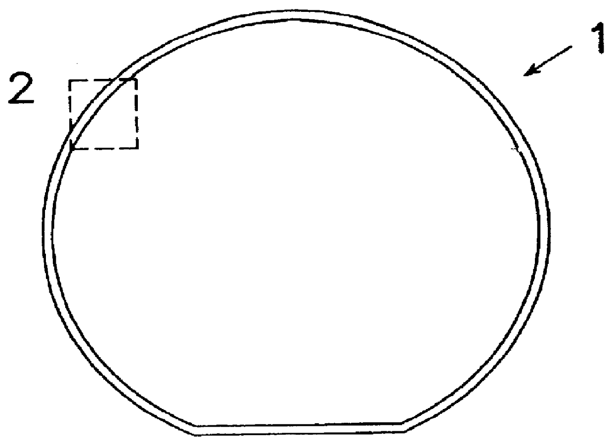
In particular, removal of the (silicon dioxide) layer in a defined edge area from the bottom of the wafer (undercutting) has been found to be a problem.
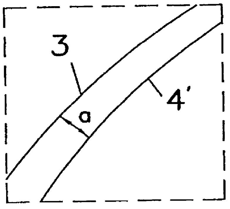
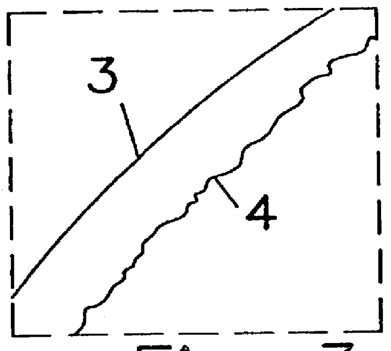
Experience has shown that to the extent (as is conventional in semiconductor production) pure diluted or also concentrated hydrofluoric acid is used for etching of a silicon dioxide layer, an optimum result is not achieved, especially in undercutting.
Specifically the edge of the silicon dioxide layer which remains on the bottom is not a circular line, but a more or less frayed or jagged line; this is a disadvantage.
Method used
View moreImage
Smart ImageViewing Examples

Examples
example 0b
Etching medium: conc. HF; DI water 1:3
(C.sub.HF =7.3 mole / l; C.sub.x =0 mole / l; molar ratio: HF:X 1.0)
Treatment time: 75 sec.
Width of undercutting: 2.5 mm, deviation.+-.0.5 mm
example 1
Etching medium: conc. HF:glacial acetic acid:DI water 2:2:1
(C.sub.HF =14.5 mole / l; C.sub.HAC =4.4 mole / l; molar ratio: HF:HAc=3.3=roughly 10:3)
Treatment time: 25 sec.
Width of undercutting: 2.1 mm, deviation.+-.0.2 mm
example 2
Etching medium: conc. HF:glacial acetic acid:DI water=1:1:2
(C.sub.HF =7.3 mole / l; C.sub.HAC =4.4 mole / l; molar ratio: HF:HAc=1.66=roughly 5:3)
Treatment time: 50 sec.
Width of undercutting: 1.8 mm, deviation.+-.0.15 mm
Login to View More PUM
 Abstract
A process of controlled wet etching of semiconductor wafers having a silicon dioxide layer on each of two surfaces, includes entirely removing the silicon dioxide layer from a top side and selectively removing the silicon dioxide layer from the opposite side bottom in a defined area which extends to the inside from the peripheral edge of the semiconductor wafer using an etching medium which includes hydrofluoric acid or a combination of hydrofluoric acid and ammonium fluoride and at least one carboxylic acid.
Description
The invention relates to a process for wet etching of semiconductor wafers with which a layer, for example, a silicon dioxide layer, can be removed from the wafer by etching.DESCRIPTION OF THE RELATED ARTIn the production of semiconductor wafers it is often necessary to remove the (silicon dioxide) layer from one surface (top) of the wafer, from the edge of the wafer and in a defined edge area of the other surface of the wafer (bottom) by undercutting. In particular, removal of the (silicon dioxide) layer in a defined edge area from the bottom of the wafer (undercutting) has been found to be a problem. This undercutting is however necessary and must proceed in an exactly defined area, so that in the subsequent processes which are executed on the wafer and which are to be carried out as far as the edge area the (silicon dioxide) layer cannot exert any adverse effect. This is important for example when a metal layer is applied (for example, gold) to the semiconductor wafers.JP 09-1810...
Claims
Login to View More Application Information
Patent Timeline
 Patent Type & AuthorityPatents(United States)
IPC IPC(8): H01L21/02H01L21/311H01L21/308
CPCH01L21/31111
InventorSUMNITSCH, FRANZWAGNER, GERALD
OwnerLAM RES AG