

Process for synthesizing nano linear carbon array
A nano-silicon wire and array technology is applied in chemical instruments and methods, silicon compounds, inorganic chemistry, etc., to achieve the effect of reducing costs and simple preparation conditions
- Summary
- Abstract
- Description
- Claims
- Application Information
AI Technical Summary
Problems solved by technology
Method used
Image

Examples
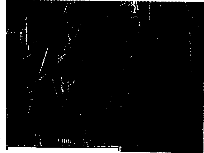
Embodiment 1
[0017] First, the reaction solution prepared to contain 5mol / l hydrofluoric acid, 0.02mol / l silver nitrate and 0.08mol / l nickel nitrate is put into the hydrothermal kettle, and the filling degree is 80%; Put the monocrystalline silicon wafer cleaned by acid and deionized water ultrasonically into the kettle; treat it at 50°C for 60 minutes, take out the kettle and wait for the kettle to cool down, open the kettle to take out the silicon wafer, and peel off the coating on its surface; The sheet is soaked and cleaned in deionized water for 3-4 times, and dried naturally to obtain the nano silicon wire array.
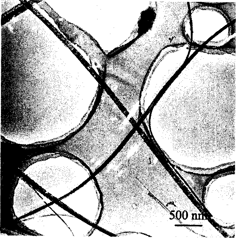
Embodiment 2
[0019] First, the reaction solution containing 5mol / l hydrofluoric acid, 0.10mol / l silver nitrate and 0.06mol / l nickel nitrate will be prepared into the hydrothermal kettle, and the filling degree is 80%; Put the monocrystalline silicon wafer cleaned by acid and deionized water ultrasonically into the kettle; treat it at 50°C for 60 minutes, take out the kettle and wait for the kettle to cool down, open the kettle to take out the silicon wafer, and peel off the coating on its surface; The silicon chip is soaked and cleaned in deionized water for 3-4 times, and then dried naturally to obtain the nano-silicon wire array.
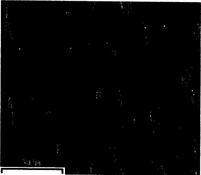
Embodiment 3
[0021] First, put the reaction solution containing 5mol / l hydrofluoric acid and 0.01mol / l silver nitrate into the hydrothermal kettle, and the filling degree is 80%; Put the processed monocrystalline silicon wafer into the kettle; treat it at 50°C for 60 minutes, take out the kettle and wait for the kettle to cool down, open the kettle to take out the silicon wafer, and peel off the coating on its surface; put the silicon wafer through deionized water for 3- After soaking and cleaning for 4 times, and drying naturally, the nano-silicon wire array is obtained.
PUM
 Abstract
Description
Claims
Application Information