Semiconductor device and method for manufacturing semiconductor device

a semiconductor device and semiconductor technology, applied in the direction of semiconductor devices, basic electric elements, electrical equipment, etc., can solve the problems of defective shape of the electrode layer and formation of an opening in the oxide semiconductor film, the failure of etching treatment, and the failure of the semiconductor device to meet the requirements of the application. the effect of reliability improvemen

Active Publication Date: 2014-01-02
SEMICON ENERGY LAB CO LTD
View PDF1 Cites 67 Cited by
  • Summary
  • Abstract
  • Description
  • Claims
  • Application Information

AI Technical Summary

Benefits of technology

[0068]When insulating films containing gallium oxide which are above and below and in contact with the oxide semiconductor film is provided so that the oxide semiconductor film is sandwiched therebetween, electrical characteristics become stable and reliability can be improved.

Problems solved by technology

However, it is difficult to perform etching treatment with a sufficiently high selectivity of the electrode layer with respect to the oxide semiconductor film.
In addition, a defective shape of the electrode layer and formation of an opening in the oxide semiconductor film might be caused depending on the etching conditions.
Such a defective shape of a semiconductor device lowers electrical characteristics.

Method used


Image

  • Semiconductor device and method for manufacturing semiconductor device
  • Semiconductor device and method for manufacturing semiconductor device
  • Semiconductor device and method for manufacturing semiconductor device

Examples


embodiment 1

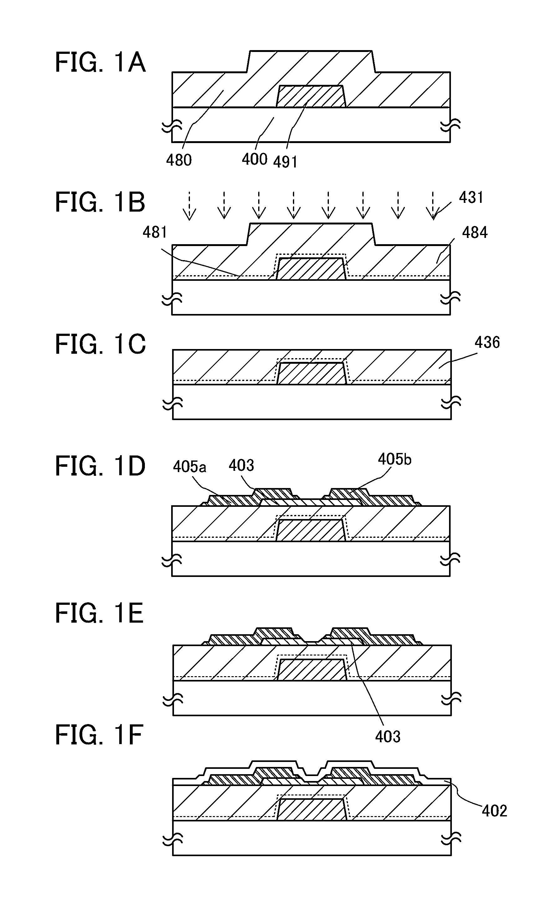
[0093]In this embodiment, one embodiment of a semiconductor device and a method for manufacturing the semiconductor device is described with reference to FIGS. 1A to 1F. In this embodiment, an example of a method for manufacturing a transistor including an oxide semiconductor film is described.

[0094]First, a conductive film is formed over a substrate 400 having an insulating surface by a sputtering method, an evaporation method, or the like, and the conductive film is etched, whereby a conductive layer 491 is formed.

[0095]There is no particular limitation on a substrate that can be used as the substrate 400 having an insulating surface as long as it has heat resistance enough to withstand heat treatment performed later. For example, a glass substrate of barium borosilicate glass, aluminoborosilicate glass, or the like, a ceramic substrate, a quartz substrate, or a sapphire substrate can be used. A single crystal semiconductor substrate or a polycrystalline semiconductor substrate of...

embodiment 2

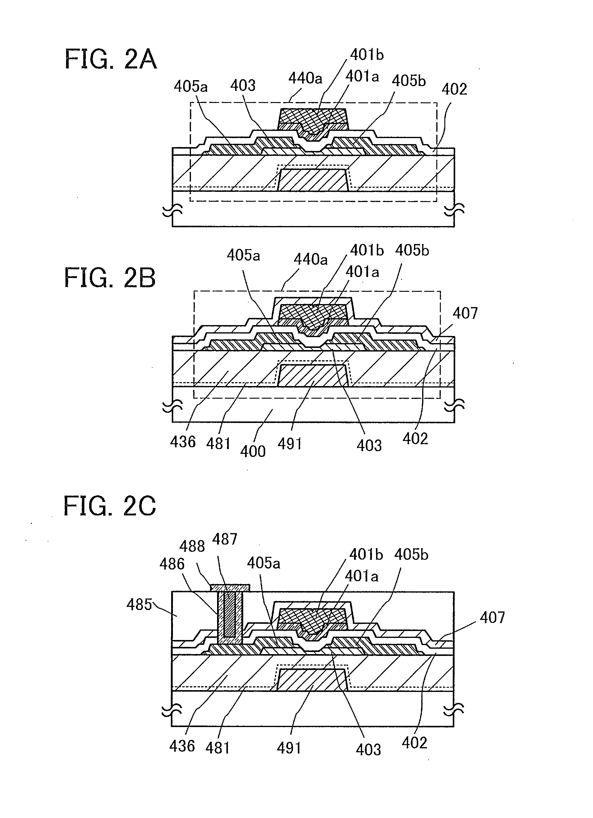
[0171]In this embodiment, an example of a method for manufacturing a transistor is described below; the method allows reduction in parasitic capacitance that is formed among a gate electrode layer, a gate insulating film, and a source electrode layer which overlaps with the gate electrode layer with the gate insulating film provided therebetween and parasitic capacitance that is formed among the gate electrode layer, the gate insulating film, and a drain electrode layer which overlaps with the gate electrode layer with the gate insulating film provided therebetween. Part of steps in a manufacturing process is the same as that in Embodiment 1, and thus the detailed description of the part of the steps is omitted.

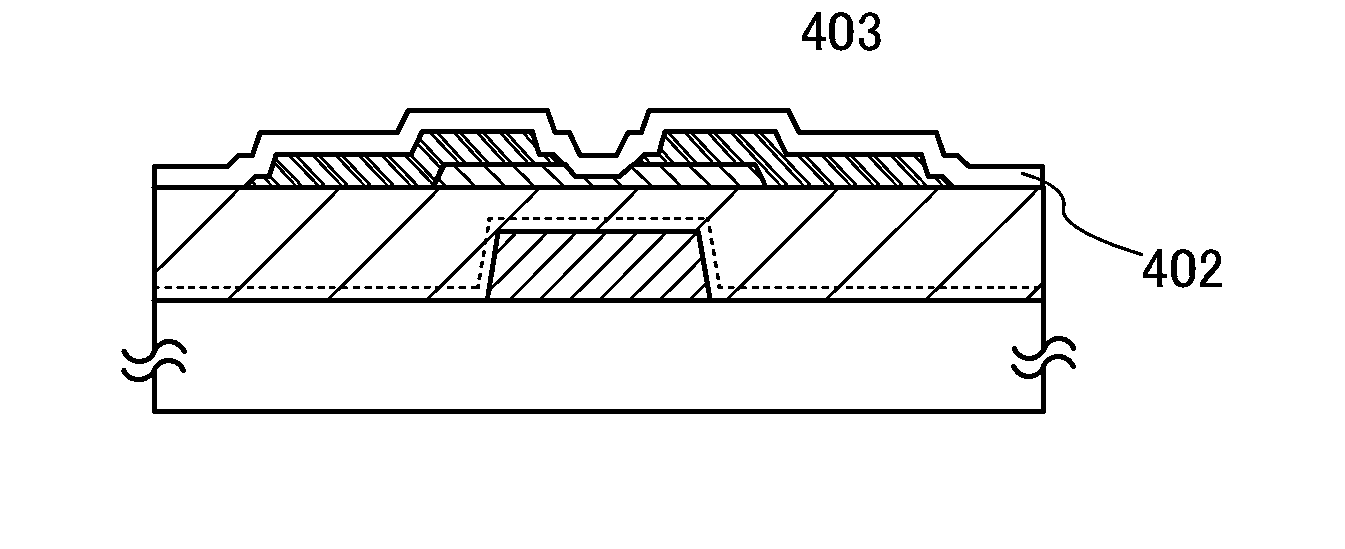
[0172]First, steps up to and including the step in FIG. 1C, which is described in Embodiment 1, are performed. That is, the conductive layer 491 is formed over the substrate 400, and the oxide insulating film 436 including the oxygen-excess region 481 is formed. A cross-secti...

embodiment 3

[0202]In this embodiment, an example of a semiconductor device including the transistors described in Embodiment 1 or 2 is described with reference to FIGS. 7A and 7B.

[0203]The semiconductor device illustrated in FIGS. 7A and 7B includes transistors 740 and 750 including a first semiconductor material in a lower portion, and a transistor 610 including a second semiconductor material in an upper portion. The transistor 610 has a structure similar to that of the transistor 441d described in Embodiment 2. The same reference numerals are used for the same parts as those in FIG. 5C. FIG. 7B is a circuit diagram of the semiconductor device in FIG. 7A.

[0204]Here, the first semiconductor material and the second semiconductor material are preferably materials having different band gaps. For example, the first semiconductor material may be a semiconductor material other than an oxide semiconductor (e.g., silicon) and the second semiconductor material may be an oxide semiconductor. A transisto...


PUM


Abstract

Provided is a method for manufacturing a transistor by which the defective shape of a semiconductor device is prevented in the case where a source electrode layer and a drain electrode layer are formed on an oxide semiconductor film. A source electrode layer and a drain electrode layer are formed each having a cross-sectional shape with which disconnection of a gate insulating film is unlikely to occur even when the gate insulating film over the source electrode layer and the drain electrode layer has a small thickness. An oxide semiconductor film having a crystal structure over an insulating surface is formed; an electrode layer on the oxide semiconductor film is formed; and a thickness of an exposed portion of the oxide semiconductor film is reduced by exposing the oxide semiconductor film to dilute hydrofluoric acid with a concentration higher than 0.0001% and lower than or equal to 0.25%.

Description

BACKGROUND OF THE INVENTION[0001]1. Field of the Invention[0002]The present invention relates to a semiconductor device including an oxide semiconductor and a method for manufacturing the semiconductor device.[0003]In this specification, a semiconductor device generally means a device which can function by utilizing semiconductor characteristics, and an electrooptic device, a semiconductor circuit, and an electronic device are all semiconductor devices.[0004]2. Description of the Related Art[0005]A technique for manufacturing a transistor or the like including an oxide semiconductor film for a channel formation region and applying it to a display device has been attracting attention. Examples of such a transistor include a transistor in which zinc oxide (ZnO) is used for an oxide semiconductor film and a transistor in which InGaO3(ZnO), is used for an oxide semiconductor film. A technique for manufacturing such a transistor including an oxide semiconductor film over a light-transmit...

Claims


Application Information

Patent Timeline
Patent Type & Authority Applications(United States)
IPC IPC(8): H01L29/66
CPCH01L29/66969H01L29/78648H01L29/7869H01L29/78696H01L21/3063H01L29/66742H01L21/465H01L29/66772
Inventor SASAGAWA, SHINYAFUJIKI, HIROSHI
Owner SEMICON ENERGY LAB CO LTD
Why Eureka
Try Eureka