Noise suppression circuits for suppressing noises above and below reference voltages

a noise suppression circuit and reference voltage technology, applied in the field of electronic circuits, can solve the problems of false switching events, increased switching time of signal lines, and increased switching time of line-to-line interconnect coupling

Inactive Publication Date: 2001-01-30
IBM CORP
View PDF5 Cites 11 Cited by
  • Summary
  • Abstract
  • Description
  • Claims
  • Application Information

AI Technical Summary

Problems solved by technology

As a result, there will be an increase in switching time for the signal line.
Furthermore, line-to-line interconnect coupling can also cause noise.
Noises that are above ground and below power supply can cause false switching events

Method used


Image

  • Noise suppression circuits for suppressing noises above and below reference voltages
  • Noise suppression circuits for suppressing noises above and below reference voltages
  • Noise suppression circuits for suppressing noises above and below reference voltages

Examples


Embodiment Construction

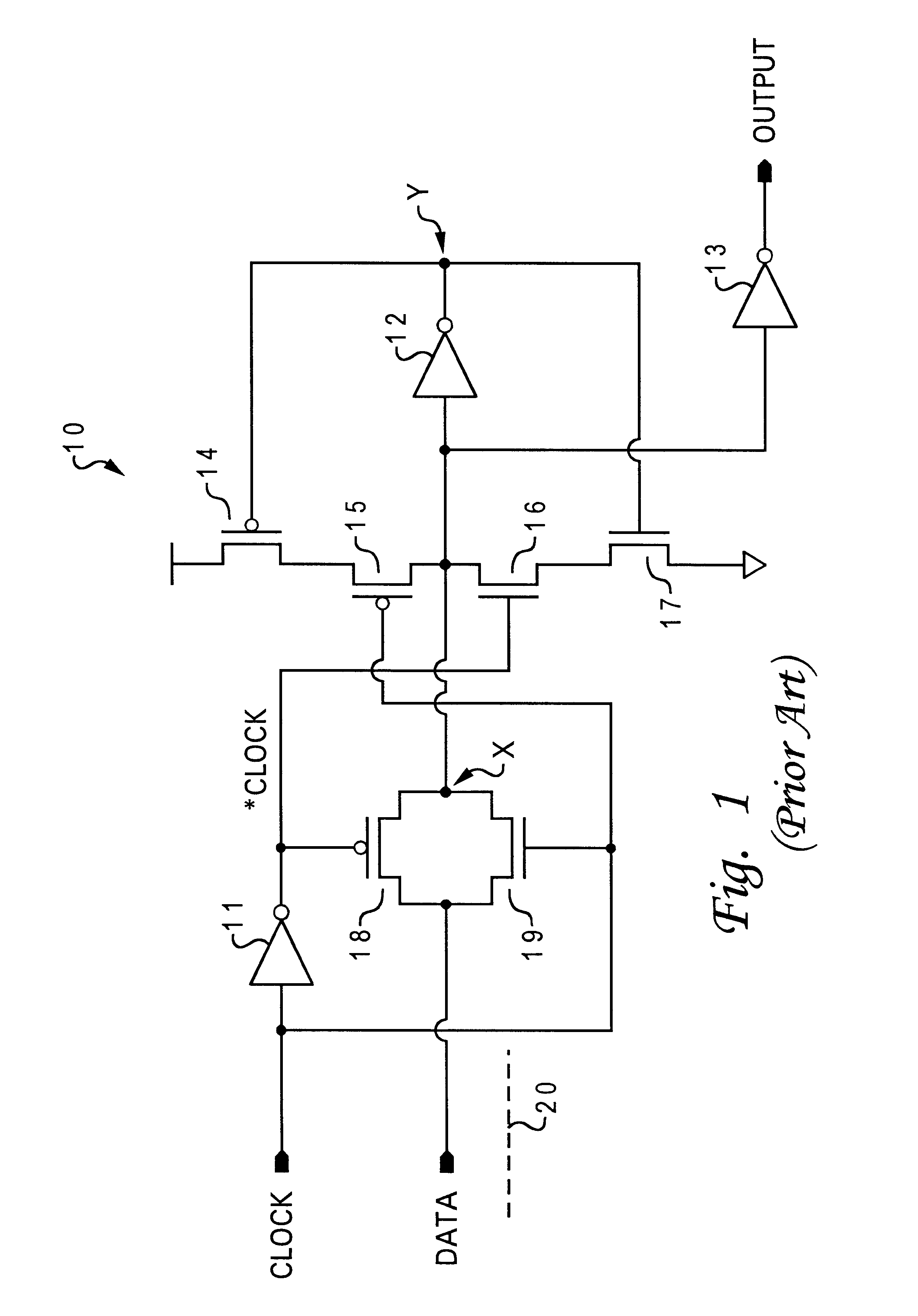
The present invention can be illustrated via a conventional latch circuit. Referring now to the drawings and in particular to FIG. 1, there is illustrated a circuit diagram of a conventional latch circuit. As shown, latch circuit 10 includes inverters 11-13 and transistors 14-19. Latch circuit 10 also includes a clock input, a data input, and an output. Typically, when the clock signal is low, the state of the data input is stored in node X. When the clock signal is high, the state of node X (i.e., the previous state of the data input) is allowed to pass through to the output (with an inversion).

For example, when the clock signal is high and the *clock signal is low, p-channel transistor 18 and n-channel transistor 19 are turned on, which allows the data input to propagate to node X. Additionally, the high clock signal turns off p-channel transistor 15 and the low *clock signal turns off n-channel transistor 16, breaking the feedback loop from node Y to node X. Thus, inverter 12 can...


PUM


Abstract

A noise suppression circuit for suppressing noises above and below reference voltages is disclosed. The noise suppression circuit for suppressing noises includes a means for generating a power-on-reset signal, a clamping transistor, and a feedback circuit. The means for generating a power-on-reset signal presets an internal latch of the noise suppression circuit to a predetermined state, such as a logical high state. The clamping transistor restores the state of a data input of a circuit to which the noise suppression circuit is providing protection, after the occurrence of a noise coupling event. The feedback circuit then turns off the clamping transistor after a predetermined amount of time.

Description

1. Technical FieldThe present invention relates to electronic circuits in general, and in particular to noise suppression circuits. Still more particularly, the present invention relates to noise suppression circuits for suppressing above-supply and below-ground noises.2. Description of the Prior ArtAs electronic circuits continue to reduce in size, metallurgical limitations begin to have more influence on line-to-line interconnect coupling. At a minimum, line-to-line interconnect coupling can increase effective load capacitance if a signal line is switching when a neighboring net is concurrently switching in an opposite direction from the signal line. As a result, there will be an increase in switching time for the signal line.Furthermore, line-to-line interconnect coupling can also cause noise. Generally speaking, noise can bounce in one or more of the following four distinct directions: above ground, below ground, above power supply, and below power supply. Noises that are above ...

Claims


Application Information

Patent Timeline
IPC IPC(8): H03K5/1252H03K3/00H03K19/003H03K3/356H03K5/125H03K17/22H04L25/08
CPCH03K3/356008H03K5/1252H03K17/223H03K19/00361H04L25/08
Inventor DURHAM, CHRISTOPHER MCCALLKLIM, PETER JUERGEN
Owner IBM CORP
Why Eureka
Try Eureka