Multilayer printed circuit board having a concave metal portion

a printed circuit board and metal portion technology, applied in the direction of electrical apparatus construction details, sustainable manufacturing/processing, final product manufacturing, etc., can solve the problems of reducing the reliability of the connection, unable to obtain sufficient connection strength, and prone to deformation of photosensitive resin

Inactive Publication Date: 2001-02-06
GLOBALFOUNDRIES INC
View PDF5 Cites 22 Cited by
  • Summary
  • Abstract
  • Description
  • Claims
  • Application Information

AI Technical Summary

Problems solved by technology

Although there are other such materials, this photosensitive resin is susceptible to deformation by high temperature or high pressure.
On the other hand, if the temperature, applied when bonding is performed, is set to a low temperature in order to prevent the formation of such a depressed portion of the photosensitive resin layer 14, then there will be the problem that a sufficient connection strength cannot be obtained between the wire and the pad and therefore a reduction in reliability of the connection will be caused.

Method used


Image

  • Multilayer printed circuit board having a concave metal portion
  • Multilayer printed circuit board having a concave metal portion
  • Multilayer printed circuit board having a concave metal portion

Examples


Embodiment Construction

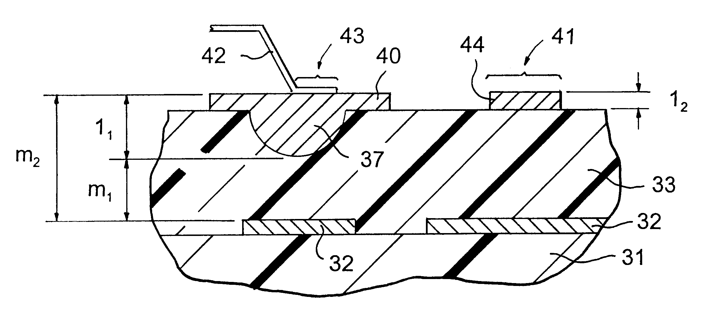
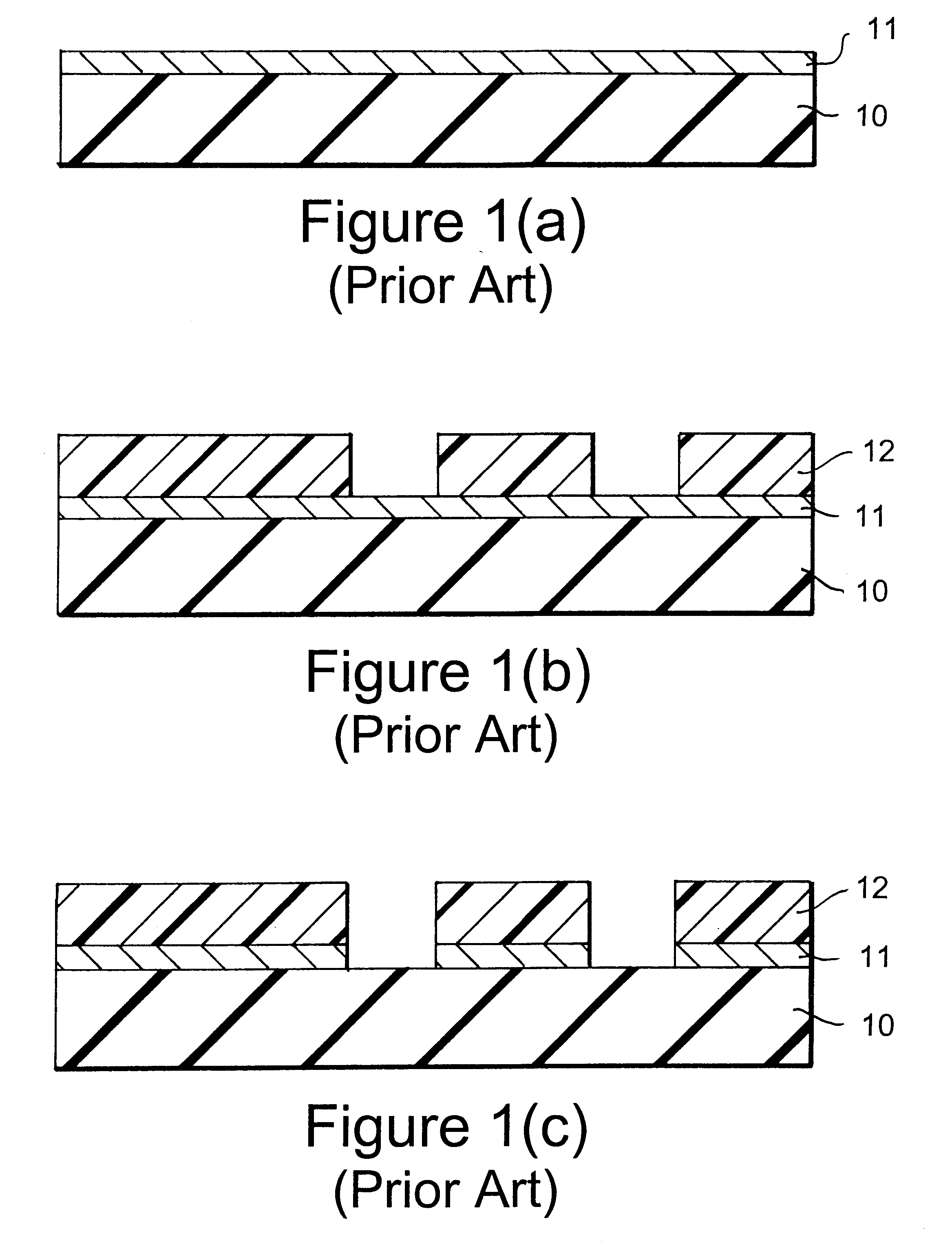
A preferred embodiment of the inventive method for fabricating a multilayer printed circuit board is described hereinbelow with reference to FIG. 3, with the resulting multilayer printed circuit board being depicted in FIG. 4. As shown in FIG. 3, in the first step of the inventive fabrication method, a blanket metal layer 32 of copper is formed on an organic substrate 31. This is achieved by using either a deposition method, such as sputtering, or an electroless plating method (FIG. 3(a)). This metal layer 32 is then patterned into a wiring layer (FIG. 3(b)). This is performed by forming a patterned photoresist on the metal layer 32, and then etching the metal layer 32 while using the patterned photoresist as an etch mask. After the etching step, the photoresist is stripped.

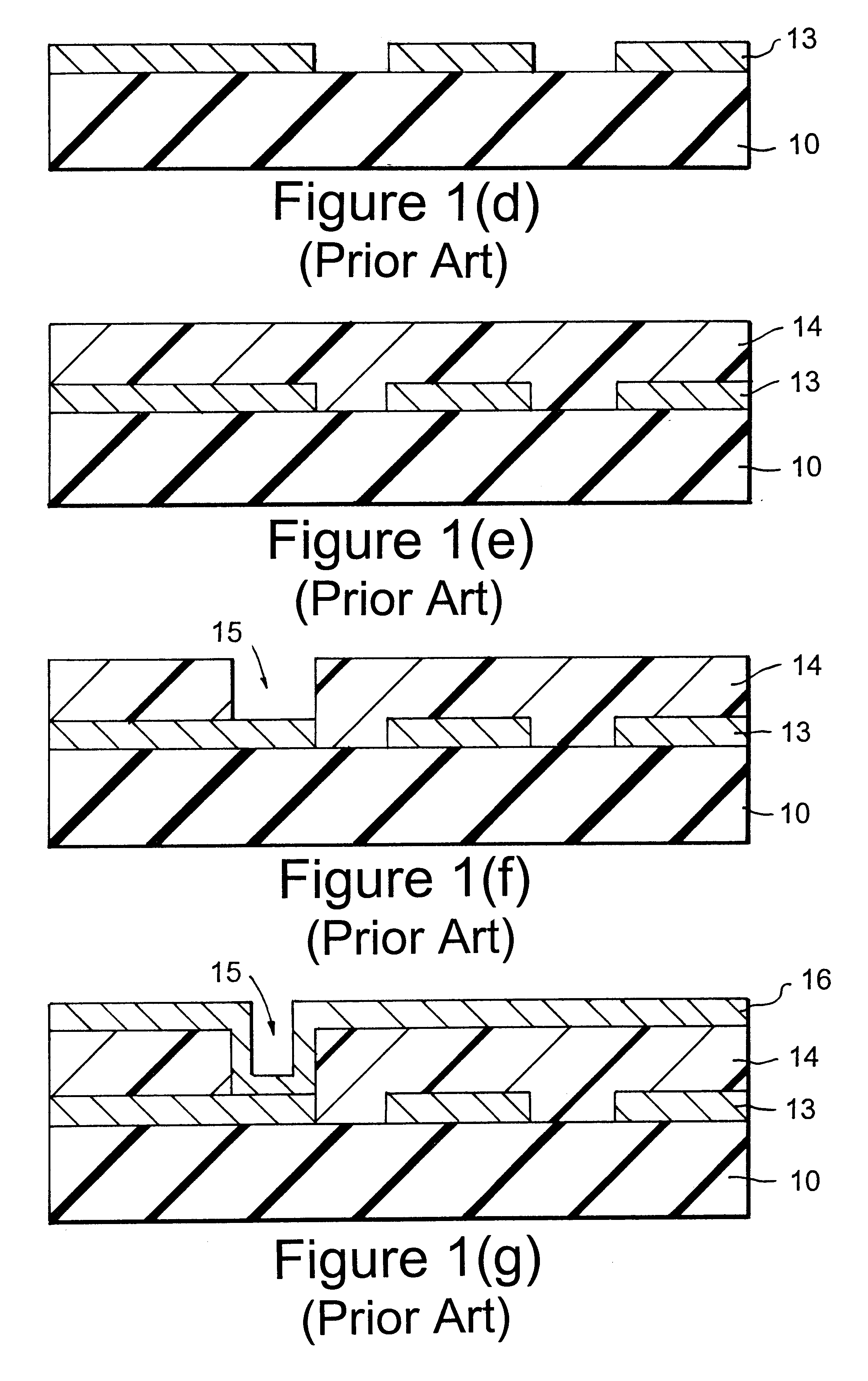
A dielectric layer 33 made of photosensitive resin is formed on the metal layer 32. Then, the photosensitive dielectric layer 33 is selectively exposed to actinic radiation and developed so that, at an area 35, a...


PUM


Abstract

The multilayer printed circuit board includes a substrate, a first conductive circuit layer, a photosensitive dielectric layer and a second conductive circuit layer which is electrically connected to the first conductive circuit layer through photo-via holes formed in the photosensitive dielectric layer. The second conductive circuit layer includes a wiring area where a plurality of wires are arranged and a pad area to which an external wire is to be connected using thermocompression bonding. Significantly, to avoid depressing the photosensitive dielectric layer underneath the pad area during the thermocompression bonding, the thickness of the second conductive circuit layer at least in the pad area, is made greater than that in the wiring area by extending this thickness into the photosensitive dielectric layer.

Description

1. Field of the InventionThe present invention relates to a multilayer printed circuit board and to a method of fabricating the multilayer printed circuit board. More particularly, the present invention relates to a multilayer printed circuit board where a plurality of wires in different wiring layers are electrically connected by via-holes and to a method of fabricating this multilayer printed circuit board.2. Background of the InventionAs electronic equipment becomes smaller and more compact, the printed circuit board on which such electronic equipment is mounted must have a larger number of wires in a limited space. This requirement can be achieved by increasing the number of circuit layers (also called wiring layers herein) of the printed circuit board and making the board into a multilayer circuit board. A plurality of such circuit layers are then connected to each other through via holes.A now conventional process for fabricating a multilayer printed circuit board is described...

Claims


Application Information

Patent Timeline
Patent Type & Authority Patents(United States)
IPC IPC(8): H05K1/11H05K3/32H05K3/00H05K3/46
CPCH05K1/111H01L24/45H01L2224/45144H01L2224/4847H01L2924/01004H01L2924/01078H01L2924/01079H05K3/0023H05K3/328H05K3/4644H05K2201/09736H01L2924/00014H01L2924/19107Y02P70/50
Inventor OKABE, SHUHICHISAKURAI, KEIZO
Owner GLOBALFOUNDRIES INC
Why Eureka
Try Eureka