Solderless pin connection

a technology of connecting pins and sockets, applied in the direction of printing element electric connection formation, lighting and heating apparatus, lighting support devices, etc., can solve the problems of unreliable connection, complex and costly manufacturing steps, waste of materials,

Inactive Publication Date: 2001-04-17
ILLINOIS TOOL WORKS INC
View PDF5 Cites 24 Cited by
  • Summary
  • Abstract
  • Description
  • Claims
  • Application Information

AI Technical Summary

Benefits of technology

As shown in FIG. 2, at least one hole 25 is drilled or punched in substrate 10 to accommodate a corresponding pin connection. Hole 25 extends from top surface 13 of substrate 10 to bottom surface 15 of substrate 10. According to one preferred embodiment of this invention, hole 25 is punched thereby reducing the complexity of the assembly process and enabling a more precise hole position.

Problems solved by technology

This subtractive manufacturing process is step intensive and results in wasted materials.
Soldered connections require additional complex and costly manufacturing steps and may result in unreliable connections.
Waste from the soldering and plating processes is hazardous to the environment and expensive to dispose of safely.
Further, manufacture of the plated through hole requires a lengthy process with many steps, including a drilled hole, that are critical to achieving a sound electrical connection.
This lengthy plating process, combined with the assembly of the pin, may jeopardize the integrity of the plated through hole.

Method used


Image

  • Solderless pin connection
  • Solderless pin connection

Examples


Embodiment Construction

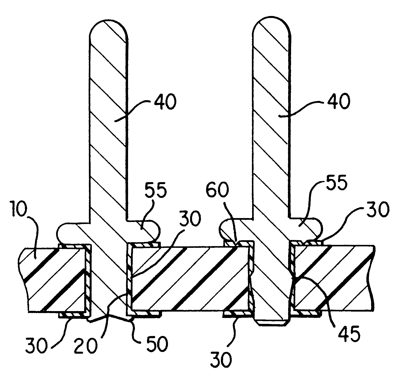
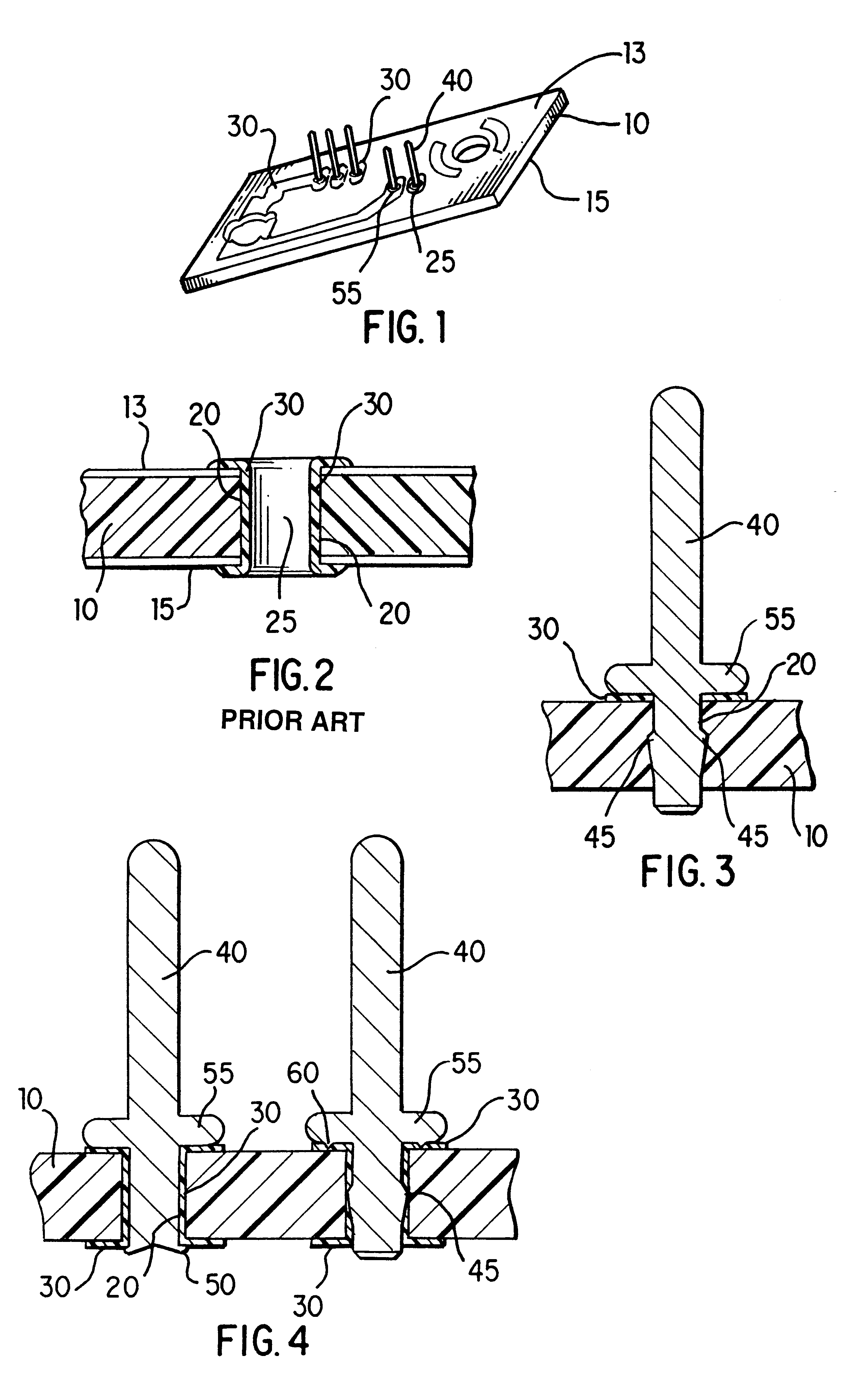
A pin connection for a printed circuit board according to this invention is shown and described that does not require copper, a plated through hole or solder. According to a preferred embodiment of this invention, polymer thick film 30 is used in connection with the printed circuit board to effectuate such a solderless connection.

Printed circuit boards are typically constructed on substrate 10 such as a fiberglass board or other substrate known to those having ordinary skill in the art. For the purpose of the Specification and claims, a printed circuit board may comprise any number of substrates 10 other than fiberglass, including plastic or other materials, because, unlike copper, polymer thick film is appropriate for use with a wide range of substrate materials. A representative printed circuit board is shown in FIG. 1.

As shown in FIG. 2, at least one hole 25 is drilled or punched in substrate 10 to accommodate a corresponding pin connection. Hole 25 extends from top surface 13 of...


PUM


Abstract

A solderless pin connection for a printed circuit board wherein a substrate is printed with polymer thick film. The substrate includes an inner surface defining a hole. The polymer thick film is applied along a top surface of the substrate and along the inner surface. The polymer thick film may additionally be applied along a bottom surface of the substrate with an additional layer along the inner surface. A pin, having a diameter less than a diameter of the hole, is press fit within the polymer thick film along the inner surface the pin. The pin is staked with respect to the substrate using a mechanical connection such as barbs or a folded portion on a staked end of the pin.

Description

1. Field of the InventionThis invention relates to a solderless pin connection utilizing a press fit pin staked within a hole printed with polymer thick film.2. Description of Related ArtTraditional printed circuit boards are manufactured by applying a layer of copper to a substrate and then etching the desired circuit into the layer of copper. This subtractive manufacturing process is step intensive and results in wasted materials. A perceived advantage of copper is its ability to maintain a soldered connection for electrical and mechanical connections. Staking a pin into a multi-processed copper plated through hole may result in a solder-free joint.Soldered connections require additional complex and costly manufacturing steps and may result in unreliable connections. Waste from the soldering and plating processes is hazardous to the environment and expensive to dispose of safely. Further, manufacture of the plated through hole requires a lengthy process with many steps, including ...

Claims


Application Information

Patent Timeline
Patent Type & Authority Patents(United States)
IPC IPC(8): H05K3/30H05K3/40H01R12/58H05K1/11H05K3/32
CPCH01R12/58H05K3/308H05K3/4069H05K2201/09981H05K2201/10303H05K2201/1059H05K2201/10871Y10S439/931F21V21/08
Inventor CUBON, MICHAEL M.
Owner ILLINOIS TOOL WORKS INC
Why Eureka
Try Eureka