Charge compensator for voltage regulator

a voltage regulator and compensator technology, applied in pulse manipulation, pulse technique, instruments, etc., can solve the problems of insufficient charge supply of charge compensators, inability to properly compensate for variations in operating conditions of semiconductor devices, and the size of semiconductors to increase,

Inactive Publication Date: 2001-04-24
SAMSUNG ELECTRONICS CO LTD
View PDF3 Cites 29 Cited by
  • Summary
  • Abstract
  • Description
  • Claims
  • Application Information

AI Technical Summary

Problems solved by technology

As a result, the voltage regulator needs a larger area due to the need for more current, and it causes the size of semiconductors to increase.
However, since conventional charge compensators are designed only in consideration of variations in state of the load connected to the voltage regulator output, there is a problem that the charge drawn through the voltage regulator output cannot be properly compensated for variations in operating conditions of a semiconductor device.
Nonetheless, the conventional charge compensators are designed regardless of such operating conditions, so that the charge compensators cannot provide an appropriate amount of charge sufficient for compensating for the variations in the operating conditions of a semiconductor.

Method used


Image

  • Charge compensator for voltage regulator
  • Charge compensator for voltage regulator
  • Charge compensator for voltage regulator

Examples


Embodiment Construction

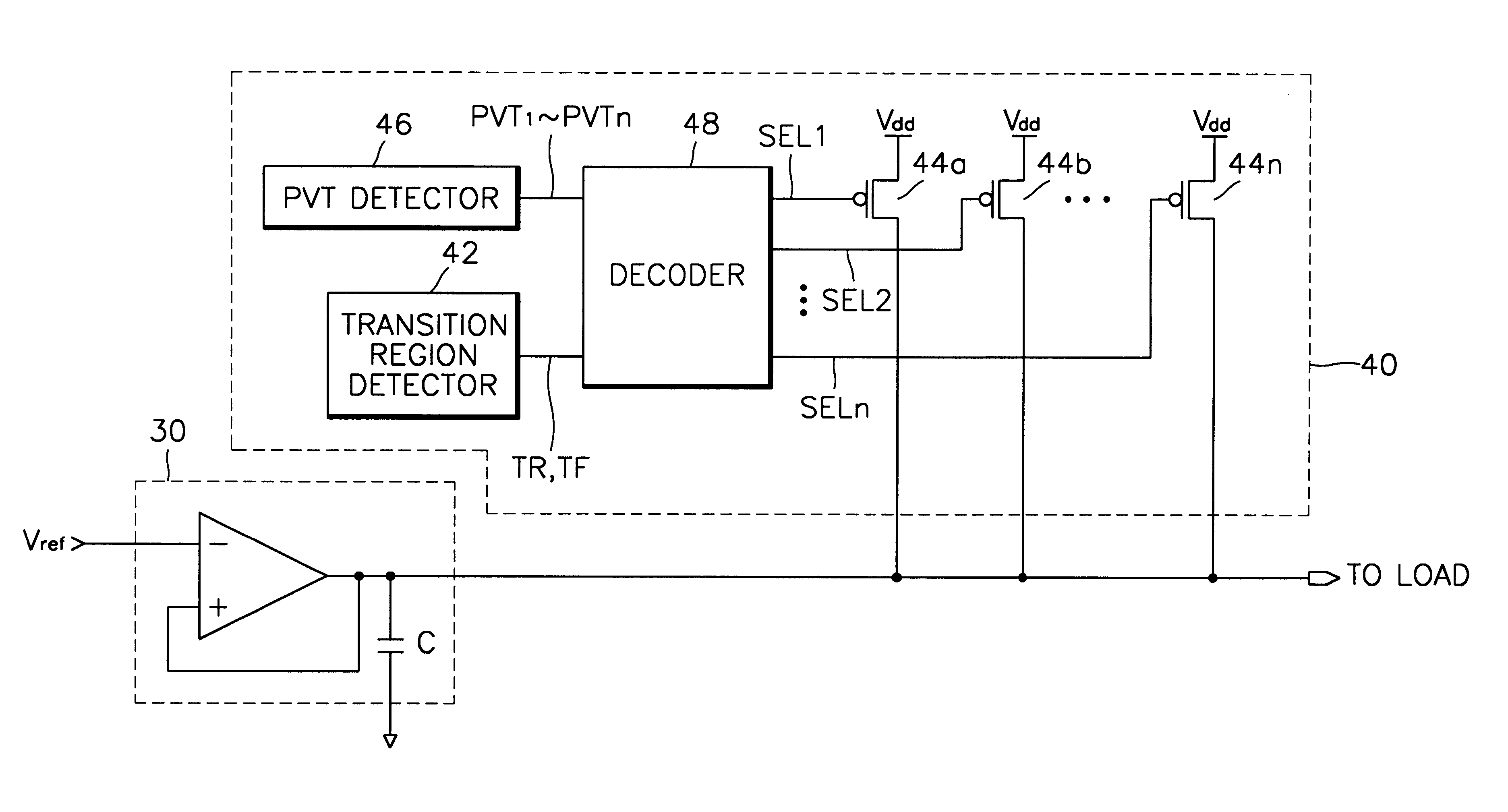
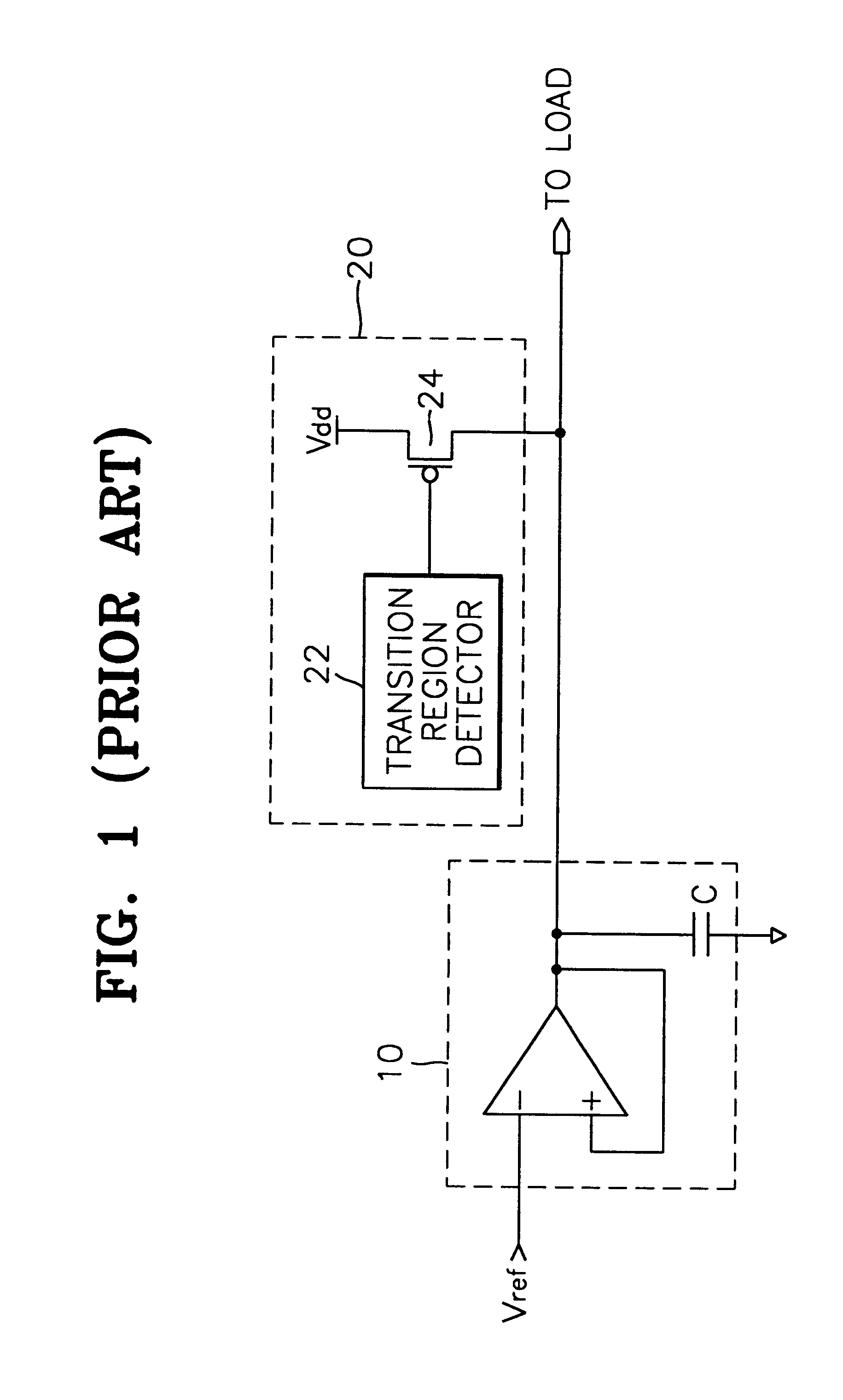
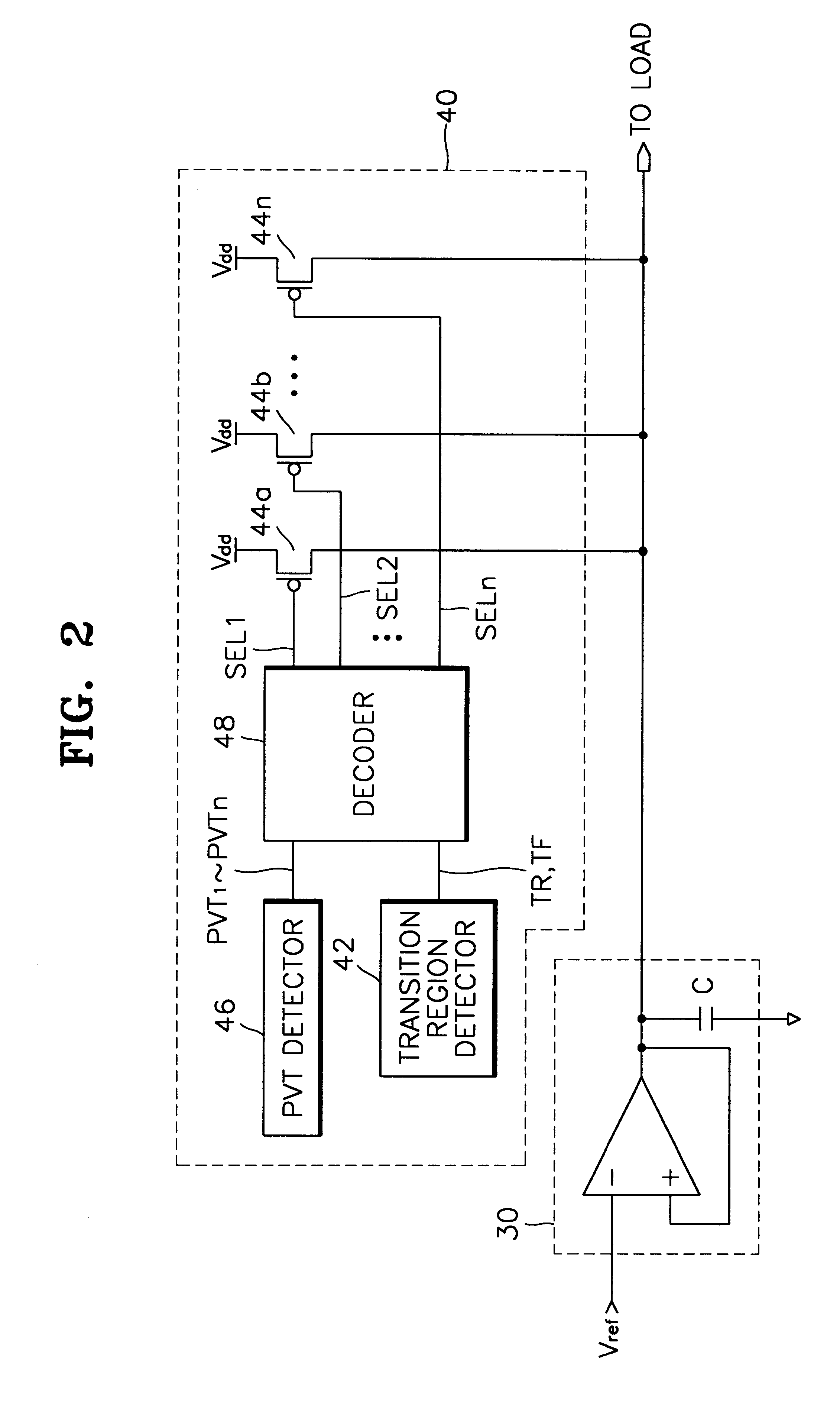
In FIG. 1, reference numeral 10 represents a voltage regulator for generating a reference voltage and reference numeral 20 represents a conventional charge compensator. The charge compensator 20 includes a transition region detector 22 and a pass transistor 24. The transition region detector 22 detects a transition region of a load (not shown) connected to an output of the voltage regulator 10. At the transition region, more charge is consumed by the load. An output voltage of the voltage regulator 10 is maintained at a reference voltage level by compensating the charge drawn by the load connected to the voltage regulator output. When the transition region is detected by the transition region detector 22, the pass transistor 24 turns on to supply the charge from a power supply source Vdd to the load.

In a semiconductor device, individual elements therein are sensitive to variations operating conditions of the semiconductor, such as a manufacturing process, a voltage in use and an ope...


PUM


Abstract

A charge compensator for a voltage regulator of a semiconductor device includes a process/voltage/temperature (PVT) detector for detecting characteristics of the semiconductor device varying dependent on a manufacturing process, a voltage in use and an operating temperature of the semiconductor device and for outputting state signals representing the detected characteristics; a plurality of pass transistors for providing charge to the load, connected between a power supply voltage and the output of the voltage regulator; and a decoder for selectively driving the plurality of pass transistors based on the state signals from the PVT detector. The charge compensator adjusts the amount of charge supplied to the voltage regulator in accordance with variations of the PVT characteristics, thereby suppressing voltage fluctuations in the output of the voltage regulator.

Description

1. Field of the InventionThe present invention relates to a charge compensator for a voltage regulator in a semiconductor device, and more particularly, to an improved charge compensator for adjusting charge compensation in accordance with characteristics of a semiconductor device.2. Description of the Related ArtSemiconductor devices need a voltage regulator which is able to generate electric potential of an analog level and to provide appropriate charge required for supplying the generated potential. A voltage regulator generally includes a comparator which detects a difference between an output voltage to a load and a reference voltage, and feeds back the difference to an input of the comparator to maintain the output voltage at the reference voltage level. A gain of the comparator and a feedback speed of the voltage regulator depend on amount of charge drawn per unit time through the output of the voltage regulator. As more charge is drawn through the output of the voltage regul...

Claims


Application Information

Patent Timeline
Patent Type & Authority Patents(United States)
IPC IPC(8): G05F3/08G05F3/24G05F1/10
CPCG05F3/242G05F1/10
Inventor SONG, KI-WHAN
Owner SAMSUNG ELECTRONICS CO LTD
Why Eureka
Try Eureka