Semiconductor memory device capable of accurate control of internally produced power supply potential

a memory device and semiconductor technology, applied in the direction of digital storage, instruments, electrical equipment, etc., can solve the problems of increased current consumption of the vpp level detection circuit, difficult to use external power supply potential, and restricted gate area

Inactive Publication Date: 2001-05-08
RENESAS ELECTRONICS CORP
View PDF4 Cites 118 Cited by
  • Summary
  • Abstract
  • Description
  • Claims
  • Application Information

AI Technical Summary

Problems solved by technology

However, in view of reliability of a transistor, it is difficult to use external power supply potential ext.Vdd as a drive power supply potential of transistors without lowering it, although a low potential is used as external power supply potential ext.Vdd.
Increase in speed of response of the Vpp level detecting circuit results in increase in current consumption of the Vpp level detecting circuit.
Since boosted potential Vpp is high, a gate area may be restricted due to restrictions on reliability of the device when an MOS capacity is utilized as a capacitor used in a pump circuit.
In particular, the array structure of, e.g., an SDRAM is formed of a plurality of memory array banks, and the current consumption on the Vpp trunk line may not occur uniformly in a chip including such an array structure.
As a result, these are often located in the positions remote from consumption portions where boosted potential Vpp is used and thereby the current is actually consumed.
Therefore, such a problem arises that interconnection resistances which are present between the consumption portions and power supply circuits 920 and 930 impede smooth supply of currents.

Method used


Image

  • Semiconductor memory device capable of accurate control of internally produced power supply potential
  • Semiconductor memory device capable of accurate control of internally produced power supply potential
  • Semiconductor memory device capable of accurate control of internally produced power supply potential

Examples


first embodiment

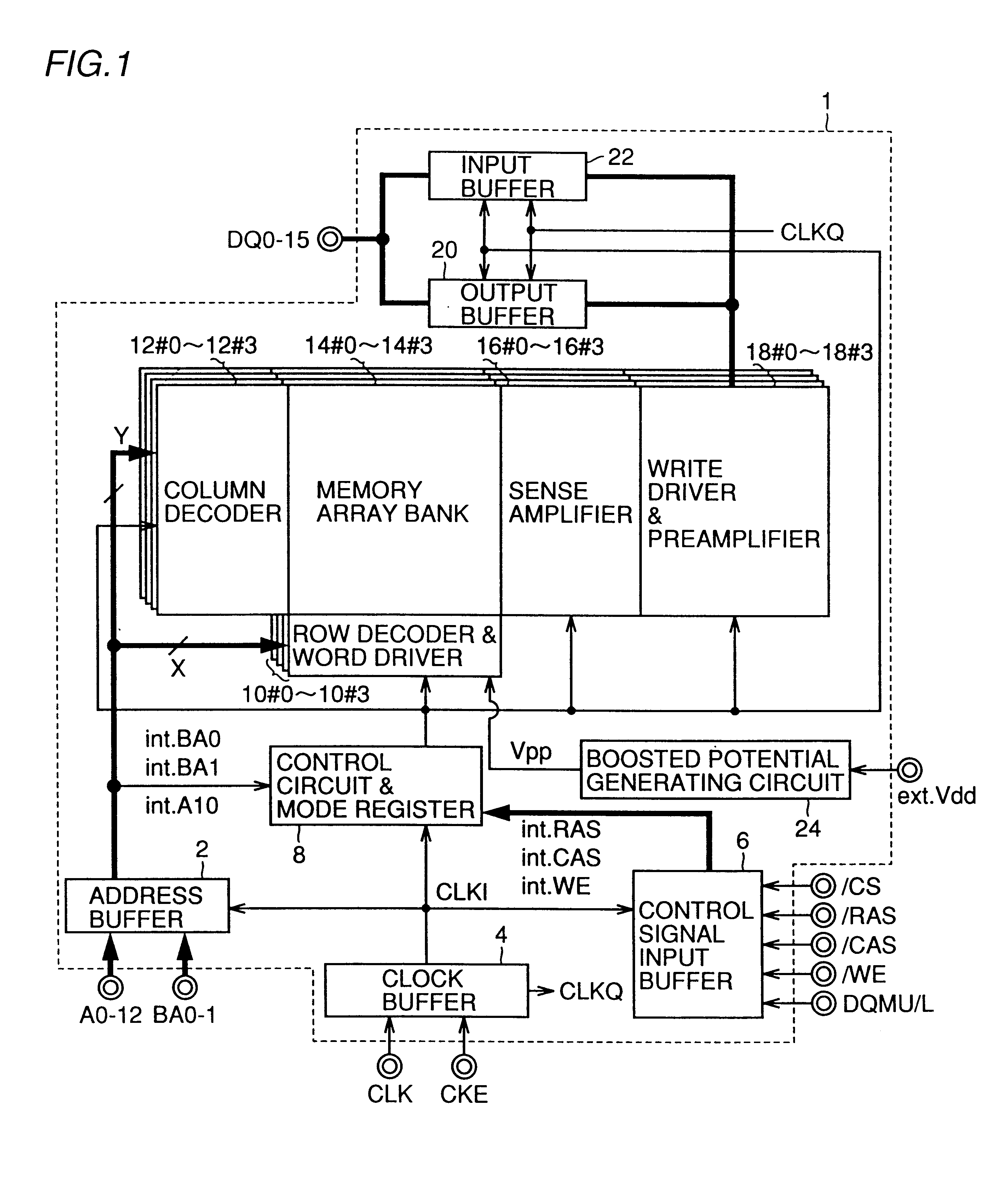
FIG. 1 is a schematic block diagram showing a structure of a semiconductor memory device 1 of the invention.

Referring to FIG. 1, semiconductor memory device 1 includes memory array banks 14#0-14#3 each having a plurality of memory cells arranged in a matrix form, an address buffer 2 which takes in externally applied address signals A0-A12 and bank address signals BA0 and BA1 in synchronization with a clock signal CLKI, and issues an internal row address, an internal column address and an internal bank address, a clock buffer 4 which receives a clock signal CLK and a clock enable signal CKE both supplied externally thereto, and issues clock signals CLKI and CLKQ to be used within the semiconductor memory device, and a control signal input buffer 6 which takes in externally applied control signals / CS, / RAS, / CAS and / WE as well as an externally applied mask signal DQMU / L in synchronization with clock signal CLKI.

Semiconductor memory device 1 also includes a control circuit which rece...

second embodiment

The first embodiment has been described in connection with the arrangement of the Vpp level detecting circuit in the multi-bank structure provided with the commonly used Vpp trunk line. Alternatively, a plurality of Vpp trunk lines which are not mutually connected may be present.

FIG. 12 shows an arrangement of a plurality of Vpp trunk lines which are not mutually connected.

Referring to FIG. 12, a semiconductor memory device 360 has a rectangular substrate. Semiconductor memory device 360 includes memory array banks 362a, 362b, 362c and 362d, which are arranged in two rows and two columns, and each have a rectangular form.

Central region CRS extends along a line connecting mid-points of the opposite short sides of the chip, and contains a region between memory array banks 362a and 362b as well as a region between memory array banks 362c and 362d. Vref generating circuit 386, Vpp level detecting circuit 388 and 384, boosted potential pump circuits 382 and 390 are arranged in central re...

third embodiment

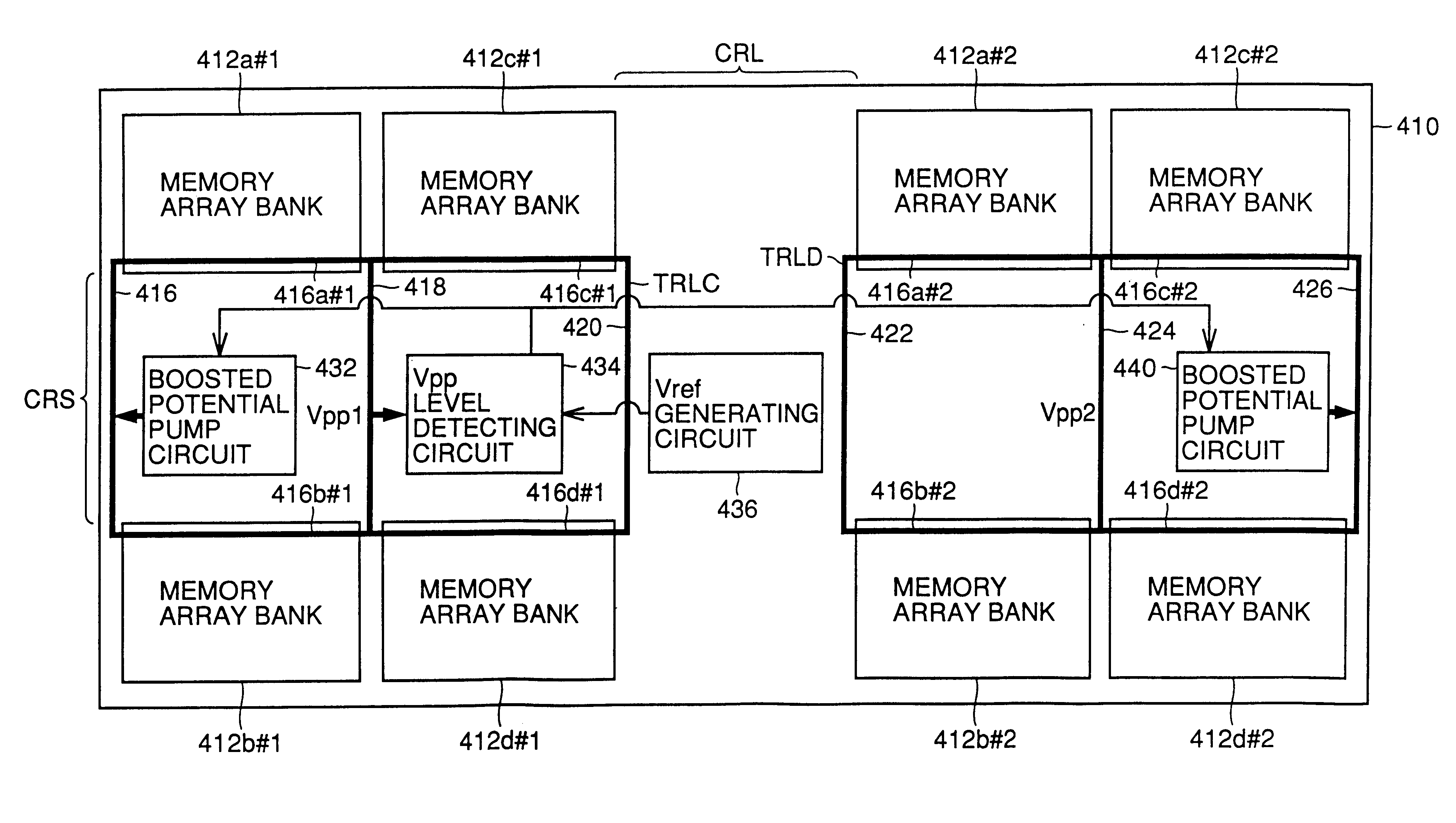
Even in the structure provided with a plurality of Vpp trunk lines which are not connected together, the Vpp level detecting circuit may be commonly used.

FIG. 13 shows an arrangement of a Vpp level detecting circuit which is commonly used.

Referring to FIG. 13, a semiconductor memory device 410 includes two Vpp trunk lines TRLC and TRLD which are independent of each other. However, each of four memory array banks 412a-412d is divided into two. Vpp trunk line TRLC is connected to corresponding divided sub-banks 412a#1-412d#1 of the respective banks, and Vpp trunk line TRLD is connected to corresponding divided sub-banks 412a#2-412d#2 of the respective banks.

For fast data transmission between the data terminals and the memory array banks, such a structure may be employed that sub-banks 412a#1-412d#l are arranged near data I / O terminals DQ0-DQ7, and sub-banks 412a#2-412d#2 are arranged near data I / O terminals DQ8-DQ15.

The divided sub-banks of the same bank are simultaneously activated. ...


PUM


Abstract

A Vpp level detecting circuit detects a potential on a Vpp trunk line which is provided commonly to a plurality of memory array banks for supplying a boosted potential thereto, and a boosted potential pump circuit supplies a current to the Vpp trunk line in accordance with a result of the detection. Since the position on the Vpp trunk line where the Vpp level detecting circuit performs the monitoring is substantially equally spaced from the respective memory blocks, an influence caused by an active state of the memory array bank can be suppressed during control of the potential on the Vpp trunk line.

Description

1. Field of the InventionThe present invention relates to a semiconductor memory device, and particularly a semiconductor memory device including a power supply circuit generating an internal power supply potential.2. Description of the Background ArtIn recent years, transistor miniaturizing technologies have been remarkably developed so that transistors mounted on a semiconductor chip have dramatically increased in number. This achieves a large capacity of a semiconductor memory device such as a Dynamic Random Access Memory (DRAM), and also achieves a one-chip structure of a memory and a logic circuit. Also, an external power supply ext.Vdd supplied to a chip can be reduced, and thereby a current consumption can be reduced. Owing to this, the device can be employed in a battery-powered instrument.However, in view of reliability of a transistor, it is difficult to use external power supply potential ext.Vdd as a drive power supply potential of transistors without lowering it, althou...

Claims


Application Information

Patent Timeline
Patent Type & Authority Patents(United States)
IPC IPC(8): G11C5/14G11C11/407G11C11/401H01L21/8242H01L27/108
CPCG11C5/145
Inventor KONO, TAKASHIMITSUI, KATSUYOSHI
Owner RENESAS ELECTRONICS CORP
Why Eureka
Try Eureka