Reset signal generation circuit

a reset signal and circuit technology, applied in the direction of generating/distributing signals, digital transmission, pulse automatic control, etc., can solve the problems of delay the chip chip operation, the frequency of the internal clock signal, and the inability to guarantee the stability of the circuit operation,

Inactive Publication Date: 2001-06-26
MAGNACHIP SEMICONDUCTOR LTD
View PDF2 Cites 33 Cited by
  • Summary
  • Abstract
  • Description
  • Claims
  • Application Information

AI Technical Summary

Problems solved by technology

Because not only power supply voltage is not sufficiently ensured, but also frequency of a clock signal is not stabilized during the oscillation-stability time, stability of circuit operation cannot be guaranteed, so the chip is prevented from operating using the reset signal.
The frequency of the internal clock signal, CLK_INT, is not stable because the level of the power voltage, VCC, is not sufficient.
Such fixed oscillation-stability time may delay the start of operation of the chip unnecessarily or may not ensure an enough oscillation-stability time because the circuit cannot reflect the condition when the operating characteristic of the oscillator deteriorates.

Method used


Image

  • Reset signal generation circuit
  • Reset signal generation circuit
  • Reset signal generation circuit

Examples


Embodiment Construction

Reference will now be made in detail to the preferred embodiments of the present invention, examples of which are illustrated in the accompanying drawings.

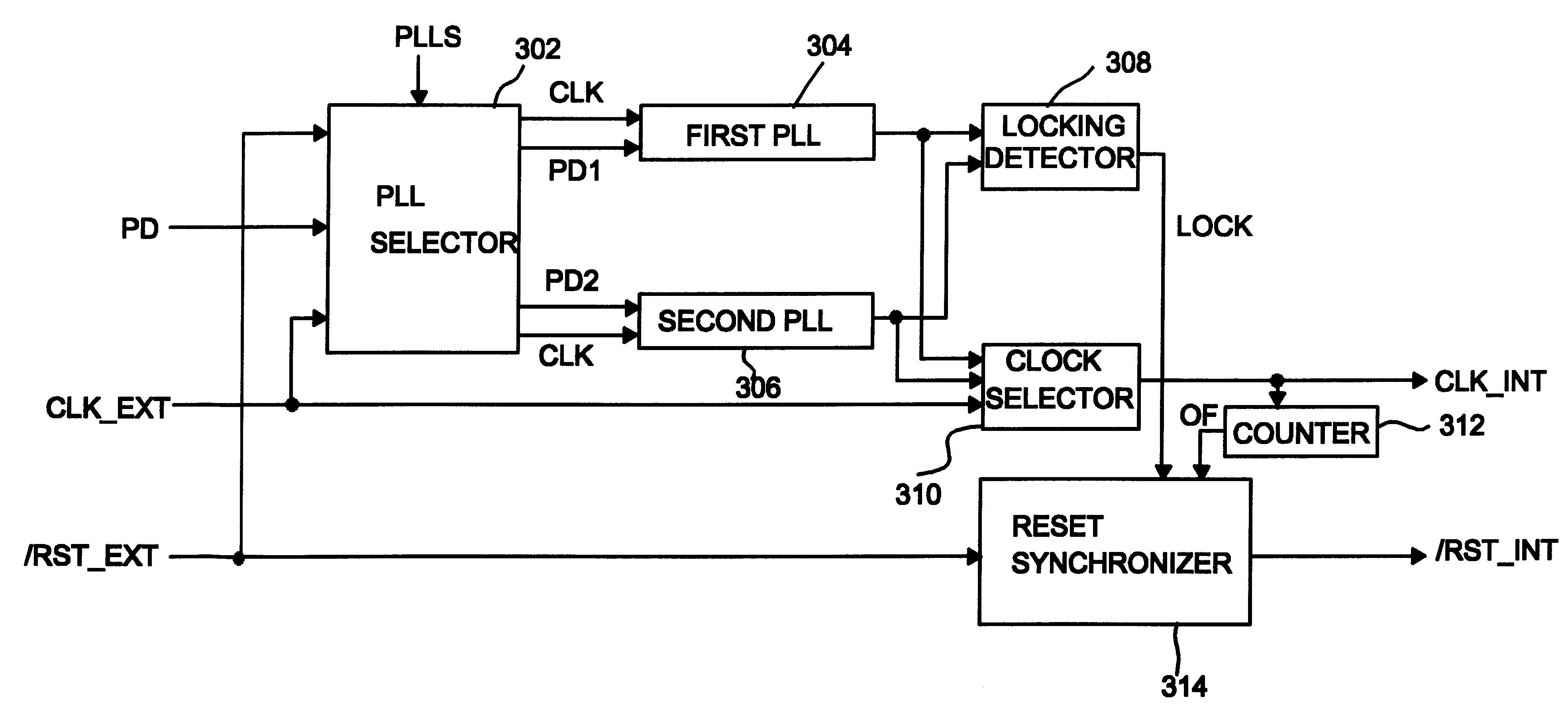
With reference to FIG. 3 and FIG. 4, the preferred embodiment of the present invention will be described.

As shown in FIG. 3, PLL selector 302 receives a power down control signal, PD, an external clock signal, CLK_EXT, an external reset signal, / RST_EXT, and a PLL selection signal, PLLS. The external reset signal, / RST_EXT, has an initial value of a low level. When the external reset signal, / RST_EXT, goes to a high level, the PLL selector is activated.

The PLL selector 302 also has a function of selecting one of two PLLs 304 and 306 that will be described below. The two PLLs 304 and 306 have different input frequency signals and different output frequency signals. Namely, one of the two PLLs is selected in accordance to a target frequency.

Each of the PLLs 304 and 306 is activated or inactivated according to the PLL selection signa...


PUM


Abstract

A reset signal generation circuit of the present invention includes a phase locked loop (PLL) selector, a plurality of PLLs, a locking detector, a clock selector, a counter, and a reset synchronizer. The PLL selector is activated when an external reset signal is high and provides a signal for selecting one of the plurality of PLLs according to a power down control signal and a PLL selection signal. The plurality of PLLs have different input frequency signals and different output frequency signals. They are activated in response to an external clock signal and inactivated in response to the power down control signal. The locking detector detects locking / unlocking of the PLLs based upon the output frequency signals of the PLLs and generates a locking signal. The clock selector selectively provides one of the output signals of the PLLs and the external clock signal. The counter is coupled to the clock selector and generates an overflow signal after completing count of a predetermined number. In response to the overflow signal of the counter, the reset synchronizer generates an internal reset signal synchronizing with the locking signal. The present invention controls the stable reset mode release time regardless of the settling time of the oscillation signal by controlling the reset signal using the locking signal of the PLL. A current state is maintained even though the locking state of the PLL is released, so the operation of the chip is not influenced by the reset of the PLL.

Description

1. Field of the InventionThe present invention relates to a clock signal generation circuit in a semiconductor chip and more particularly to a reset signal generation circuit for generating internal clock signals in a chip.2. Description of Related ArtIt takes a little time for a stable clock signal to be generated after a chip is powered and an oscillation circuit is activated. This period of time is called an oscillation-stability time. During the oscillation-stability time, reset signals are generated not to let the chip operate. Because not only power supply voltage is not sufficiently ensured, but also frequency of a clock signal is not stabilized during the oscillation-stability time, stability of circuit operation cannot be guaranteed, so the chip is prevented from operating using the reset signal.FIG. 1 is a block diagram of a related art reset signal generation circuit.Oscillator 102 performs oscillating operation in response to an incoming external clock signal, CLK_EXT.Cl...

Claims


Application Information

Patent Timeline
Patent Type & Authority Patents(United States)
IPC IPC(8): G06F1/24H03L7/07H03L7/095H03L7/08G06F1/04H03K17/00H03L7/22
CPCG06F1/24H03L7/07H03L7/095H03K17/00
Inventor LEE, KANG-BOK
Owner MAGNACHIP SEMICONDUCTOR LTD
Why Eureka
Try Eureka