Semiconductor disk device

a technology of semiconductor disk and disk unit, which is applied in the direction of redundant data error correction, input/output to record carriers, instruments, etc., can solve the problems of untimely error correction, increased firmware burden, and increased probability of deciding whether the written data is uncorrectable, etc., and achieves high speed

Inactive Publication Date: 2001-07-03
LAPIS SEMICON CO LTD
View PDF6 Cites 77 Cited by
  • Summary
  • Abstract
  • Description
  • Claims
  • Application Information

AI Technical Summary

Benefits of technology

Accordingly, it is an object of the invention to provide the semiconductor disk unit capable of realizing the error correction at high speed.

Problems solved by technology

That is, if the number of an occurrences of error bit is about 2 bits or 3 bits, a burden imposed on the firmware increases.
Further, even in the error correction by the firmware, if there is an error bit more than 4 bits in one sector data, the error correction can not be executed.
As a result, the probability of deciding whether the written data is uncorrectable increases.
Still further, there has been known such characteristics that if the semiconductor disk unit repeats data write / read operation more than given times, the probability of occurrence of error bit increases sharply.
However, if such substituting processing frequently occurs, it is prone to deteriorate a high access speed which is a feature of the semiconductor disk unit.
Further, if more substituting storage area is secured, more storage capacity of the flash EEPROM increases, thereby impeding the miniaturization of the semiconductor disk unit and entaining the increase of cost.

Method used


Image

  • Semiconductor disk device
  • Semiconductor disk device
  • Semiconductor disk device

Examples


first embodiment

[FIGS. 1 to 6]

A semiconductor disk unit according to a first embodiment of the invention will be now described with reference to FIGS. 1 to 6.

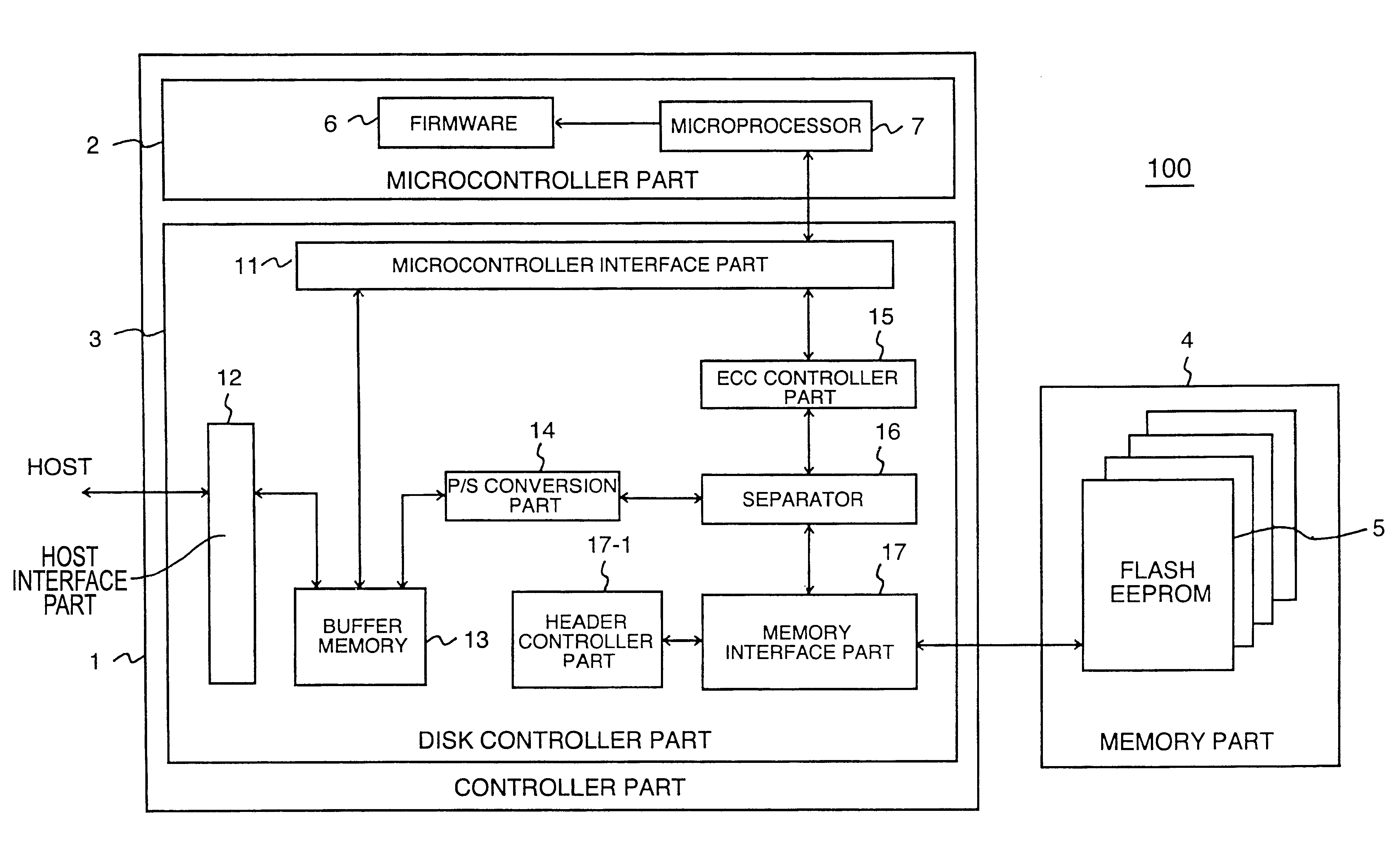
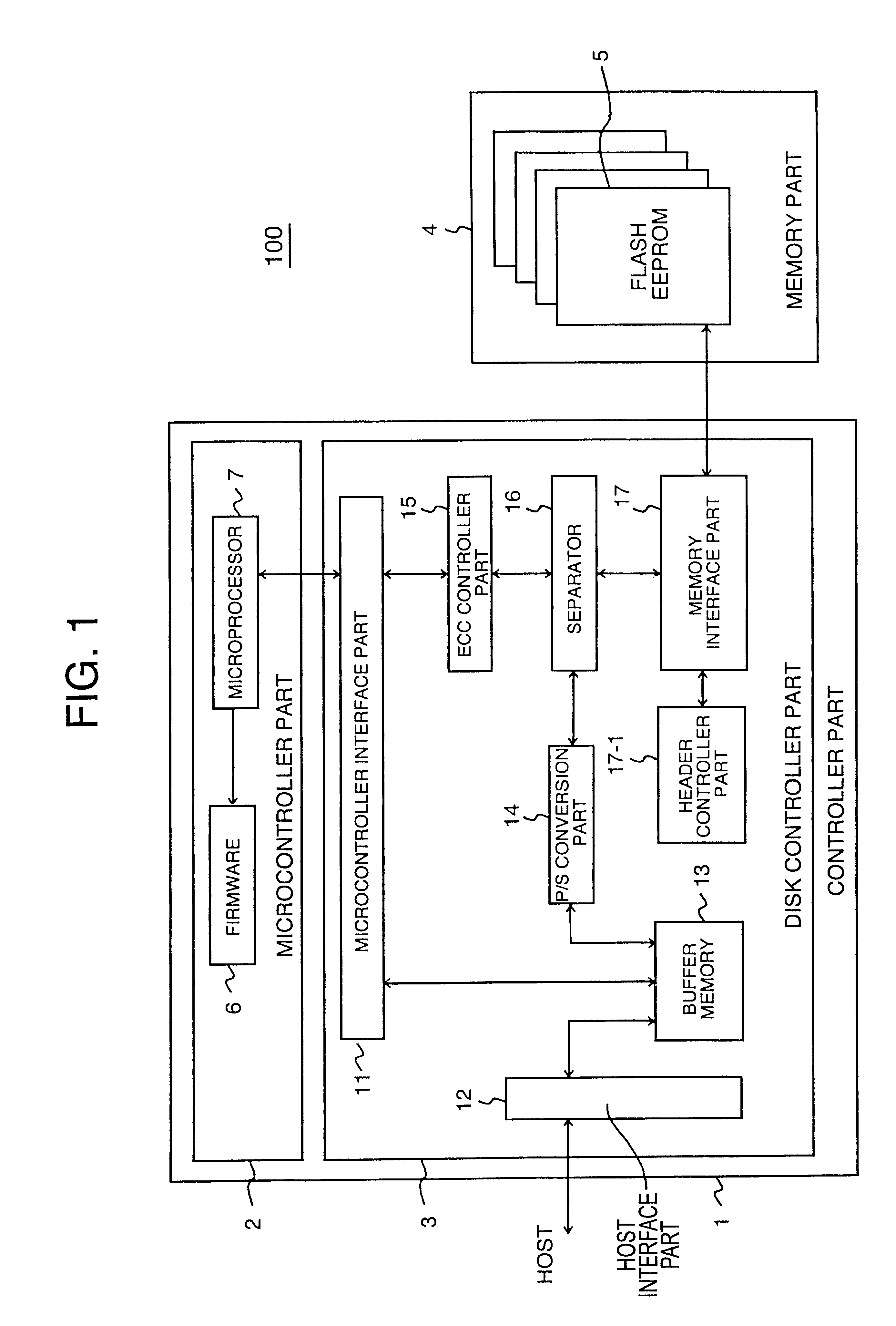
FIG. 1 is a block diagram showing the construction of the semiconductor disk unit according to the first embodiment of the invention.

In FIG. 1, a semiconductor disk unit 100 comprises a controller part 1 and a memory part 4. The controller part 1 controls data write / read processing relative to the memory part 4 which comprises a plurality of flash EEPROMs 5.

The controller part 1 comprises a microcontroller part 2 and a disk controller part 3. The microcontroller part 2 executes error correction processing if there are plurality of error bits in data or controls write / read processing relative to the disk controller part 3.

The microcontroller part 2 comprises a firmware 6 and a microprocessor 7. The firmware 6 is a program for executing an error correction processing. The microprocessor 7 reads the program of the firmware 6 for executing an erro...

second embodiment

[FIGS. 7 to 9]

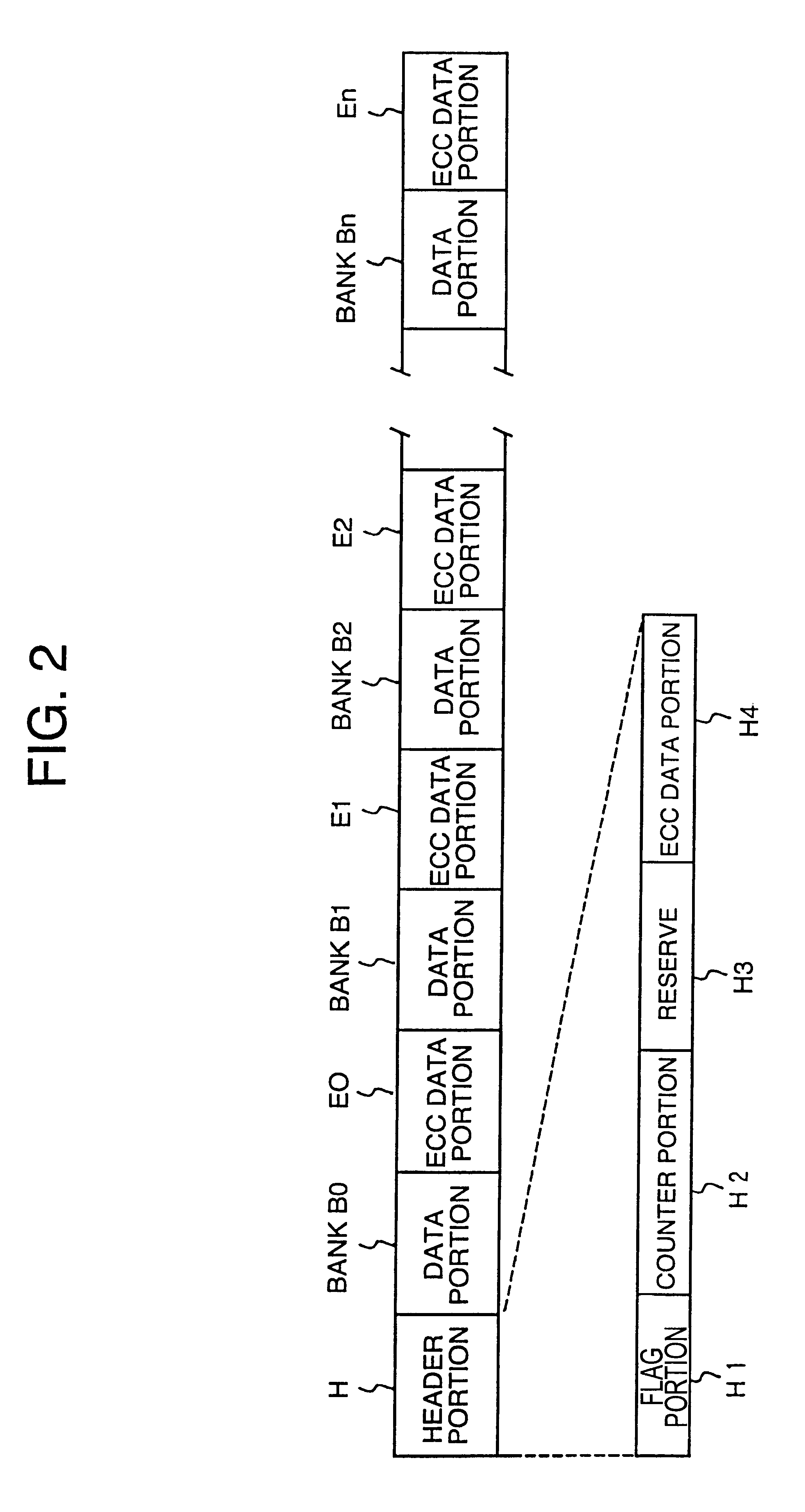
A semiconductor disk unit according to a second embodiment will be now described with reference to FIGS. 7 to 9. Since the bit width which is subjected to the preparation of the ECC data becomes a unit bank in the first embodiment, there is a probability of needing the design for a new ECC controller part. Accordingly, the second embodiment can attain the same effect as the first embodiment using the ECC controller parts for preparing the ECC data relative to one sector bit width.

FIG. 7 is a block diagram showing the construction of a semiconductor disk unit 200 according to the second embodiment of the invention. Components which are the same as those of the first embodiment are denoted by the same reference numerals.

In FIG. 7, a microcontroller part 2 and a memory part 4 are the same as those of the first embodiment. In a disk controller part 3, a microcontroller interface part 11, a host interface part 12, a buffer memory 13, a P / S conversion part 14, a memory inter...


PUM


Abstract

In a semiconductor disk unit, one sector data to be stored in a memory part is divided into a plurality of banks, and ECC data is prepared every bank so as to enhance the function of correcting errors even if there occur many error bits.

Description

TECHNICAL FIELDThe invention relates to a semiconductor disk unit, particularly to a semiconductor disk unit having functions of detecting errors and of correcting errors when stored data is read.BACKGROUND TECHNOLOGYA demand for a semiconductor disk unit has been recently increased instead of a magnetic disk unit. The semiconductor disk unit is a non-volatile semiconductor memory such as a flash EEPROM which can electrically erase data at one time, namely, by the batch, and operates like the magnetic disk unit. The semiconductor disk unit has a disadvantage in a storage capacity and a cost thereof compared with the magnetic disk unit, but it has an advantage in high access speed and miniaturization thereof.The operation of the semiconductor disk unit, particularly the write / read operation of data will be now described.First, a host transfers data to be written to a semiconductor disk unit. The semiconductor disk unit writes received data on an incorporated flash EEPROM. The write o...

Claims


Application Information

Patent Timeline
Patent Type & Authority Patents(United States)
IPC IPC(8): G06F11/10G11C29/00G06F12/16G06F3/06
CPCG06F11/1068G11C29/88G11C29/765G06F3/06
Inventor BEPPU, ATSUSHI
Owner LAPIS SEMICON CO LTD
Why Eureka
Try Eureka