Forming steep lateral doping distribution at source/drain junctions

Inactive Publication Date: 2001-07-31
IBM CORP
View PDF1 Cites 171 Cited by
  • Summary
  • Abstract
  • Description
  • Claims
  • Application Information

AI Technical Summary

Benefits of technology

The present invention makes it possible to achieve improved short channel characteristics including threshold voltage (Vt) rolloff along with better scalabilit

Problems solved by technology

However, as the junction depth has been scaled down to below for example about 30 nanometers, disadvantages occur due to the reduced

Method used


Image

  • Forming steep lateral doping distribution at source/drain junctions
  • Forming steep lateral doping distribution at source/drain junctions
  • Forming steep lateral doping distribution at source/drain junctions

Examples


Embodiment Construction

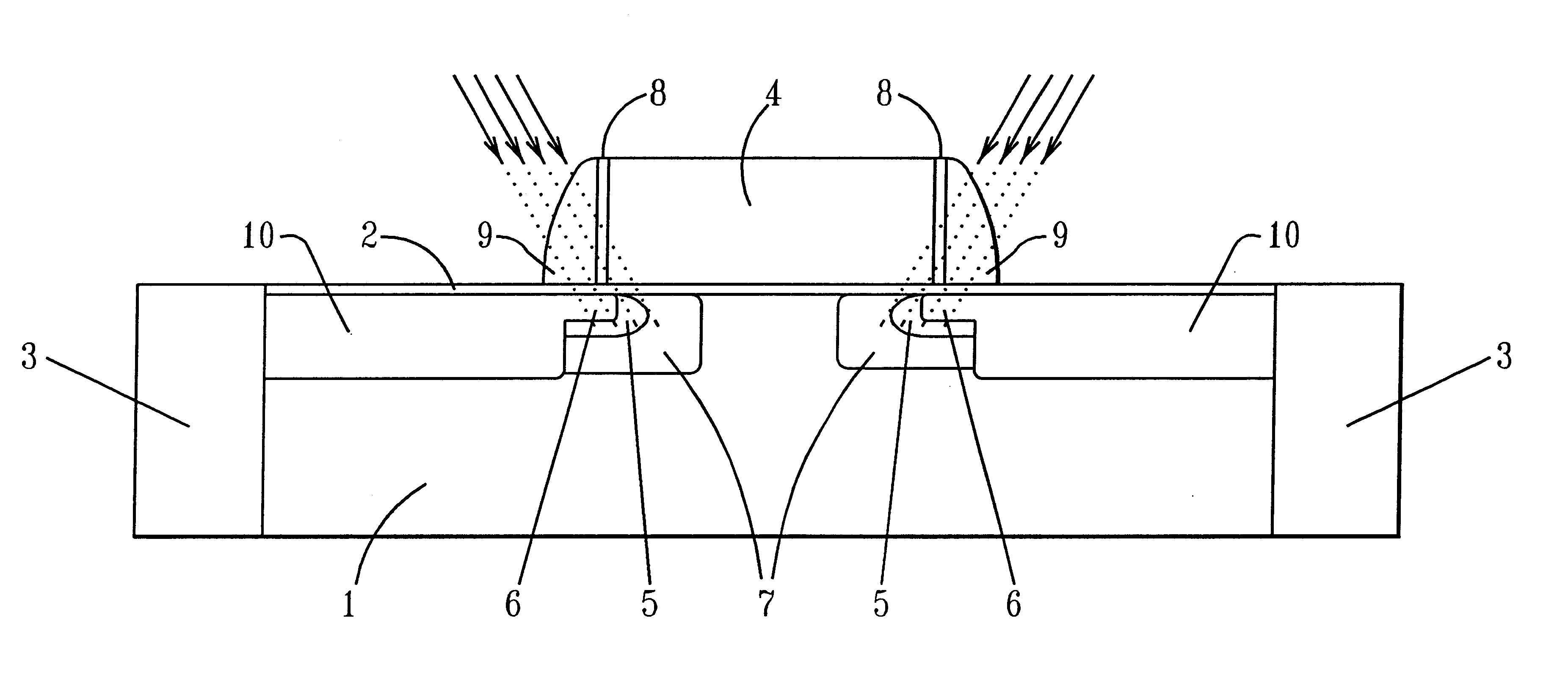
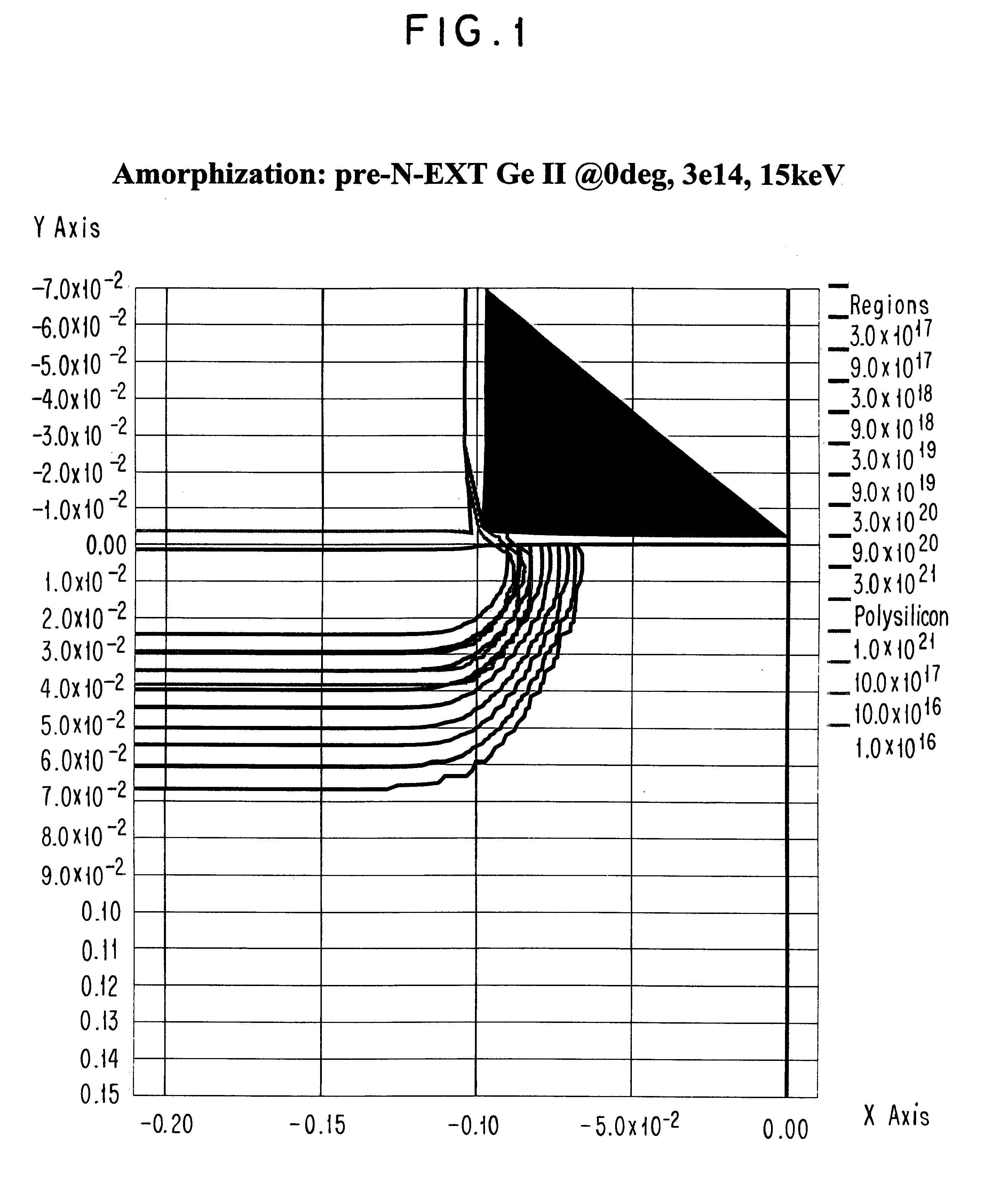
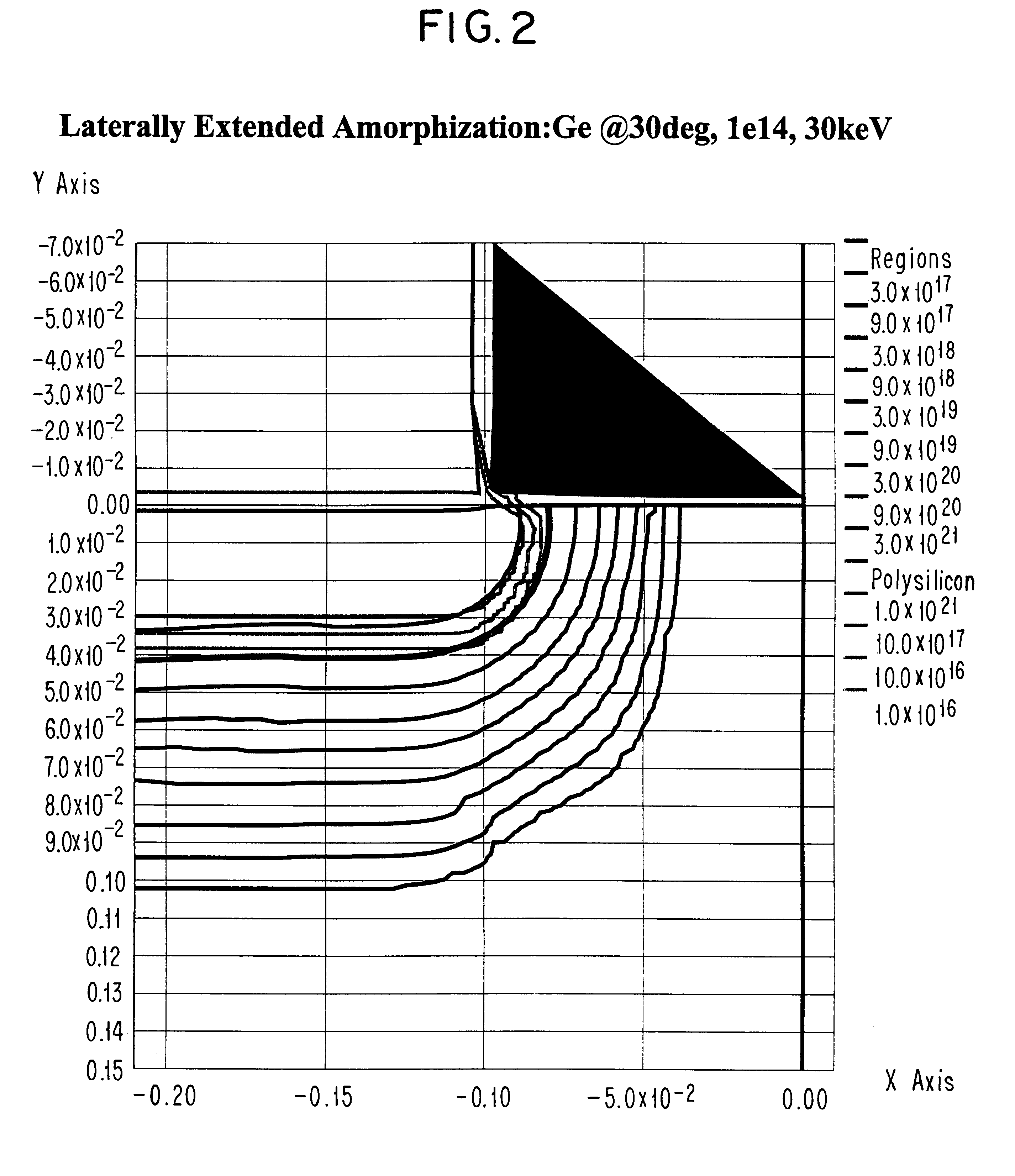
In order to facilitate an understanding of the present invention, reference will be made to the figures. For instance, when the discussion of the fabricating steps of the present invention refers to a particular type of substrate and / or a particular type of dopant impurity, it is understood that the present invention is applicable to the opposite type without departing from the spirit of the present invention. For instance, when reference is made to a p-type silicon substrate as the semiconductor substrate and n-type impurities as diffused or implanted dopant impurities, it is understood that an n-type substrate and p-type diffused or implanted dopant impurities are likewise suitable. In addition, it is understood that when the discussion refers to n-type impurities, the process steps are applicable to p-type impurities and vice versa. Also, when reference is made to impurities of a "first type" and to impurities of a "second type", it is understood that the "first type" refers to n...


PUM


Abstract

A semiconductor device is fabricated by implanting into a semiconductor substrate non-doping ions at a tilt angle of at least about 10° to laterally extend preamorphization of the substrate portion and then implanting into the substrate dopants for providing source/drain extensions or halo doping or both.

Description

DESCRIPTIONTechnical FieldThe present invention relates to a method for fabricating a semiconductor device and particularly a MOSFET exhibiting relatively steep lateral doping distribution at source / drain junctions. The present invention is especially advantageous in fabricating CMOS devices. The semiconductor devices of the present invention are fabricated by implanting silicon and / or germanium ions at a tilt angle along with wafer rotation in order to preamorphize the semiconductor substrate. Furthermore, the present invention relates to semiconductor devices obtained by the described fabrication technique.BACKGROUND OF INVENTIONField effect transistors (FETs) have become the dominant active device for very large scale integration (VLSI) and ultralarge scale integration (ULSI) applications in view of the high impedance, high density and low power characteristics of integrated circuit FETs.The most common configuration of FET devices is the MOSFET which typically comprises source a...

Claims


Application Information

Patent Timeline
IPC IPC(8): H01L21/02H01L29/78H01L21/336H01L21/265H01L29/66H01L29/02H01L29/10H01L21/8238H01L27/092H01L29/786
CPCH01L21/26506H01L21/26586H01L29/7836H01L29/6659H01L29/1083H01L21/265
Inventor PARK, HEEMYONGTAUR, YUANWANN, HSING-JEN C.
Owner IBM CORP
Why Eureka
Try Eureka