Method for producing a group III nitride compound semiconductor substrate

Inactive Publication Date: 2001-08-14
PANASONIC CORP
View PDF6 Cites 90 Cited by
  • Summary
  • Abstract
  • Description
  • Claims
  • Application Information

AI Technical Summary

Problems solved by technology

However, the above-described conventional method has the following problems.
Therefore, it has been difficult to obtain the GaN substrate 5 tha

Method used


Image

  • Method for producing a group III nitride compound semiconductor substrate
  • Method for producing a group III nitride compound semiconductor substrate
  • Method for producing a group III nitride compound semiconductor substrate

Examples


example 2

In Example 2, another example where a III-N semiconductor substrate was produced by the method of the present invention will be described. The method of Example 2 is different from that of Example 1 only in the method for cooling the substrate. Therefore, a duplicated description will be omitted.

The processes shown in FIGS. 4A to 4C were performed, and the GaN film 45a (thickness of 200 .mu.m) was formed on the Al.sub.0.1 Ga.sub.0.9 N layer 44 by causing crystal growth. Thereafter, the temperature of the wafer was reduced to room temperature by natural cooling for 20 minutes in the HVPE apparatus filled with a nitrogen atmosphere. Then, the temperature of the wafer was raised to 1000.degree. C. over 30 minutes in the HVPE apparatus filled with a nitrogen atmosphere. The heat cycle of cooling to room temperature after heating to 1000.degree. C. was repeated 5 times. Consequently, the GaN film 45a was separated from the Al.sub.0.1 Ga.sub.0.9 N layer 44, so that a GaN substrate 45 was ...

example 3

In Example 3, another example where a III-N semiconductor substrate was produced by the method of the present invention will be described. The method of Example 3 is different from that of Example 1 only in the method for cooling the substrate. Therefore, a duplicated description will be omitted.

The processes shown in FIGS. 4A to 4C were performed, and the GaN film 45a (thickness of 200 .mu.m) was formed on the Al.sub.0.1 Ga.sub.0.9 N layer 44 by causing crystal growth. Then, immediately after the GaN film 45a was formed by causing crystal growth, the substrate heater 58 was slid and nitrogen gas was sprayed to the wafer so as to cool the wafer rapidly (within 3 min). In this manner, the temperature of the wafer was reduced to room temperature. The GaN film 45a was separated by this cooling by nitrogen gas, so that a GaN substrate 45 was obtained. Then, the obtained GaN substrate 45 was removed from the HVPE apparatus.

The sliding of the substrate heater 58 was carried out to avoid d...

example 4

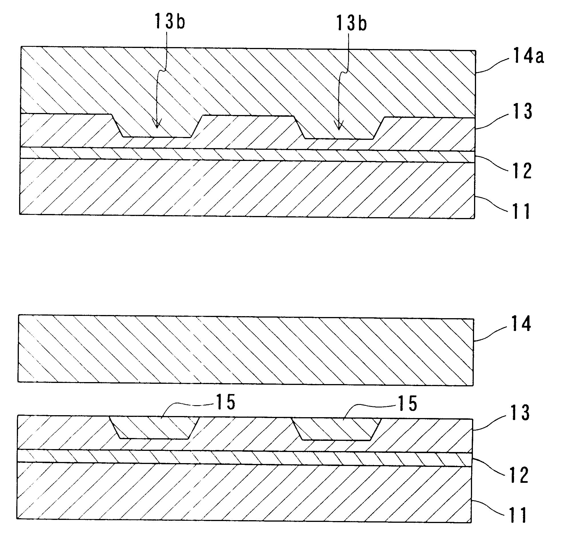
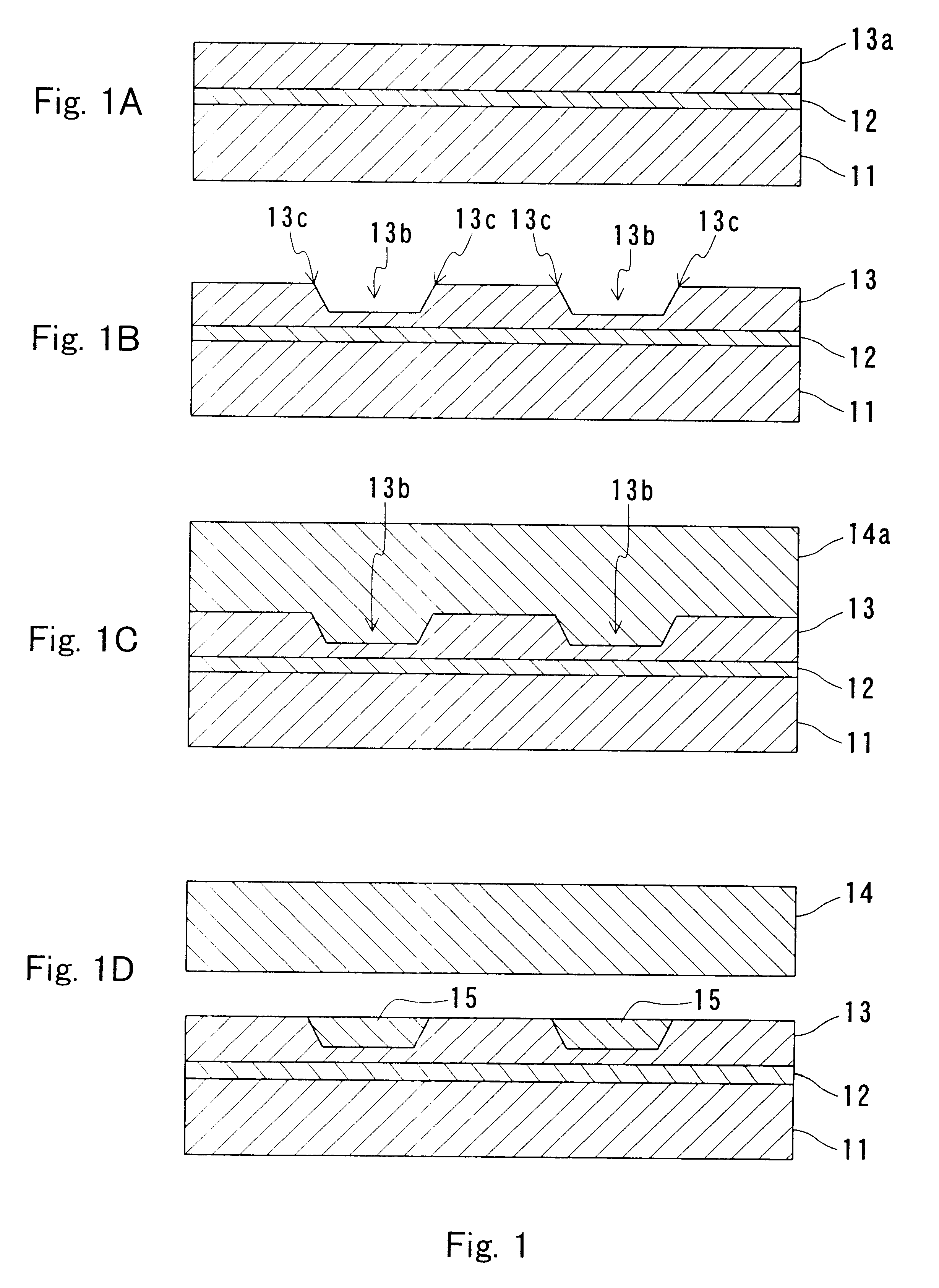
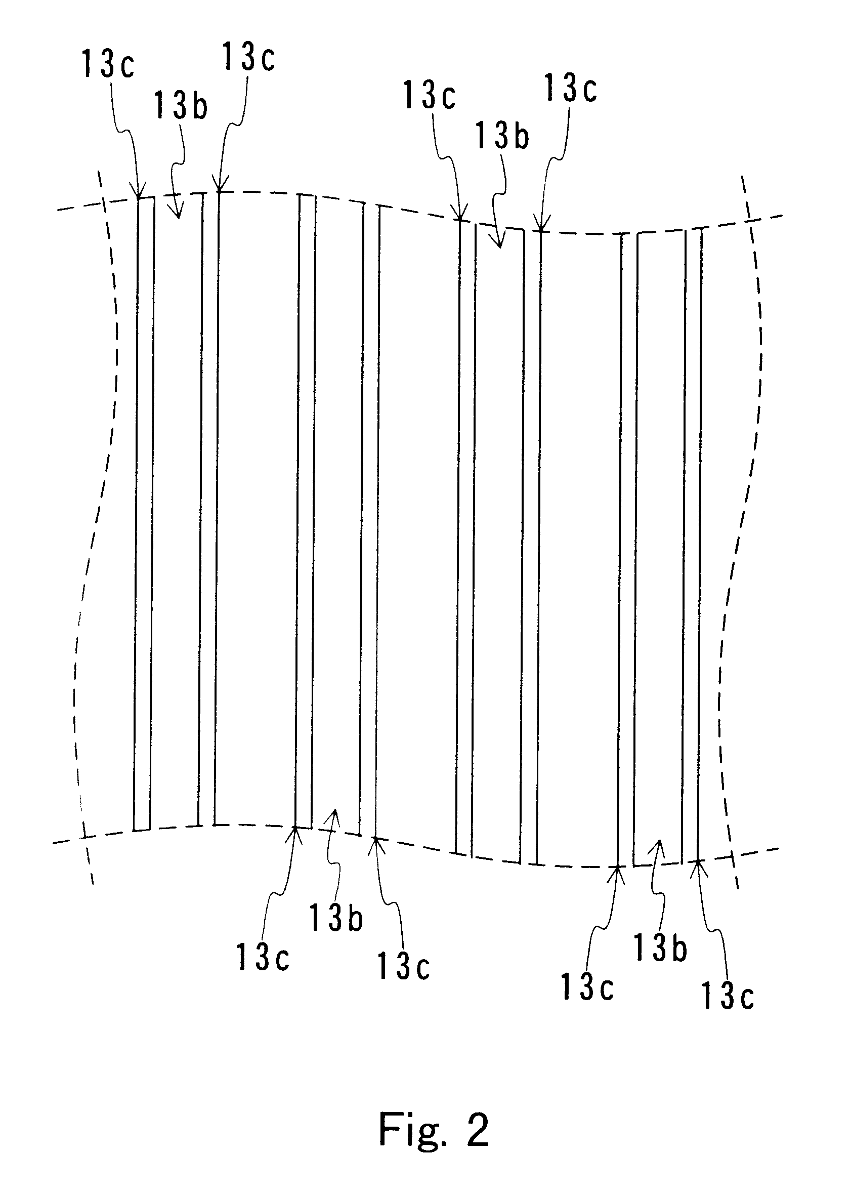
In Example 4, another example where a III-N semiconductor substrate was produced by the method of the present invention will be described with reference to FIG. 7. The method of Example 4 includes a process for forming an insulating film between the first semiconductor film and the second semiconductor film. The same description as in Example 1 will be omitted.

First, a (0001) plane sapphire substrate 41 (a diameter of 2 inches and a thickness of 300 .mu.m) was prepared and was subjected to washing, etching, and thermal cleaning in the same manner as in Example 1. Then, in the same manner as in Example 1, a GaN buffer layer 42 (a thickness of 50 nm), a GaN layer 43 (a thickness of 1 .mu.m) and an Al.sub.0.1 Ga.sub.0.9 N layer 44a (a thickness of 1 .mu.m) were formed sequentially in this order on the sapphire substrate 41 (FIG. 7A).

Next, the sapphire substrate 41 (hereinafter, also referred to as a wafer) provided with the Al.sub.0.1 Ga.sub.0.9 N layer 44a was placed in an atmospheric...


PUM


Abstract

The present invention provides a method for producing a group III nitride compound semiconductor substrate including: (a) forming a first semiconductor film over a substrate, the first semiconductor film made of a first group III nitride compound semiconductor and provided with a step; (b) forming a second semiconductor film made of a second group III nitride compound semiconductor having a different thermal expansion coefficient from that of the first group III nitride compound semiconductor on the first semiconductor film; and (c) cooling the substrate and separating the second semiconductor film from the first semiconductor film. Thus, a large-area group III nitride compound semiconductor substrate can be produced in high yields and with high reproducibility.

Description

1. Field of the InventionThe present invention relates to a method for producing a group III nitride compound semiconductor substrate.2. Description of the Prior ArtA group III nitride compound semiconductor expressed by the general formula Al.sub.X Ga.sub.1-X-Y In.sub.Y N (where 0.ltoreq.X.ltoreq.1, 0.ltoreq.Y.ltoreq.1, 0.ltoreq.X+Y.ltoreq.1) can have a band gap energy in a wide range from 1.9e V to 6.2e V. For this reason, the group III nitride compound semiconductor (hereinafter, also referred to as III-N semiconductor) is a promising semiconductor material for a light-emitting / receiving device that covers a wide range from visible light to UV rays.A large-area III-N semiconductor substrate with good quality is in demand as a substrate for producing a III-N semiconductor device. As an attempt to meet this demand, there is a conventional method for producing a III-N semiconductor substrate (reported, for example in Japanese Journal of Applied Physics Vol. 37 (1998) pp. L309-L312)....

Claims


Application Information

Patent Timeline
IPC IPC(8): H01L21/02H01L21/20H01L33/00H01L31/18H01L21/205
CPCH01L21/0237H01L21/0242H01L21/02458H01L21/02494H01L21/02502H01L21/0254H01L21/02661H01L21/02664H01L31/184H01L31/1852H01L33/0075Y02E10/544H01L21/02639Y02P70/50
Inventor YURI, MASAAKIIMAFUJI, OSAMUNAKAMURA, SHINJIISHIDA, MASAHIROORITA, KENJI
Owner PANASONIC CORP
Why Eureka
Try Eureka