Process for physical isolation of regions of a substrate board

a technology of physical isolation and substrate board, which is applied in the manufacture of solid-state devices, semiconductor/solid-state devices, electric devices, etc., can solve the problems of complex preparation of integration supports, difficult to meet the requirements of an increasingly dense integration, and difficult to meet the requirements of isolation constraints

Inactive Publication Date: 2001-10-16
COMMISSARIAT A LENERGIE ATOMIQUE ET AUX ENERGIES ALTERNATIVES
View PDF4 Cites 37 Cited by
  • Summary
  • Abstract
  • Description
  • Claims
  • Application Information

AI Technical Summary

Benefits of technology

will become more obvious from the following description with reference to the figures in the attached drawings. This description is given for illustrative purposes only and is in no way restrictive.

Problems solved by technology

Special measures taken to provide sufficient electrical isolation between components makes modifications necessary to the form of components, and frequently complex preparations of integration supports.
Furthermore, isolation constraints are frequently contrary to the requirements of an increasingly dense integration.
Isolation of more traditional electronic components formed throughout the thickness of the support substrate also involves complex substrate preparation operations.
Component isolation problems also arise for optical circuits in which it is necessary to avoid any diffusion or propagation of parasite light between the various components.
Finally, complex magnetic or mechanical isolation precautions must be taken for the manufacture of magnetic or mechanical sensors or transducers.
The difficulties mentioned above are even worse when different categories of components are to be integrated on the same substrate board, if the components have different isolation requirements.

Method used


Image

  • Process for physical isolation of regions of a substrate board
  • Process for physical isolation of regions of a substrate board
  • Process for physical isolation of regions of a substrate board

Examples


Embodiment Construction

The purpose of this invention is to propose a process for physical isolation of regions with a substrate board without the difficulties mentioned above.

One purpose in particular is to propose this type of process for making an electrical, optical, mechanical and / or magnetic isolation according to the manufacturing requirements of the circuits considered.

Another purpose is to propose such a process particularly suitable for electronic power circuits capable of providing insulation at high voltages.

Another purpose is to propose an isolation system which is easy to use, which can be implemented during or after the placement of components in or on regions of the substrate board, and which is compatible with the constraints of large scale component integration.

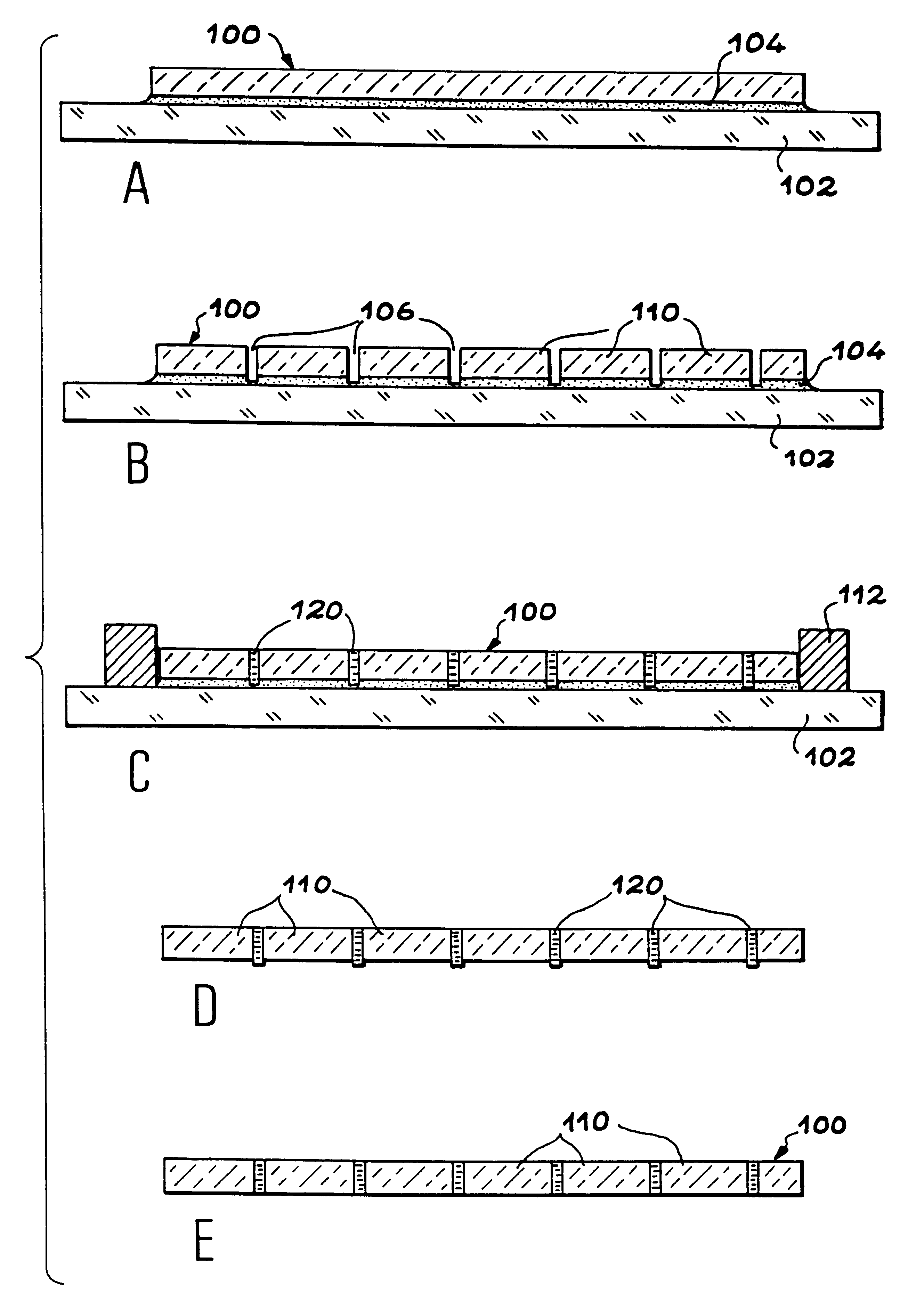
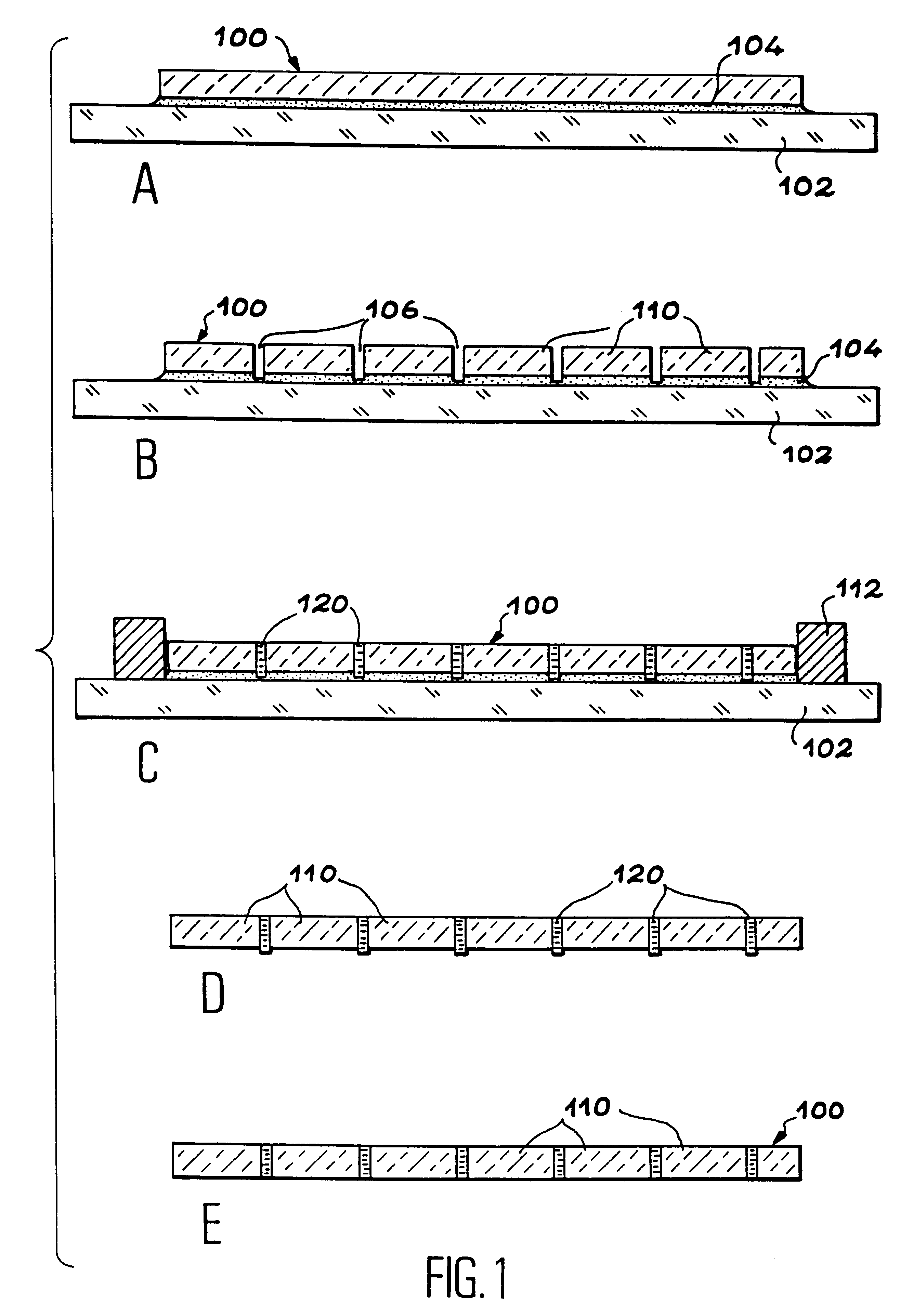
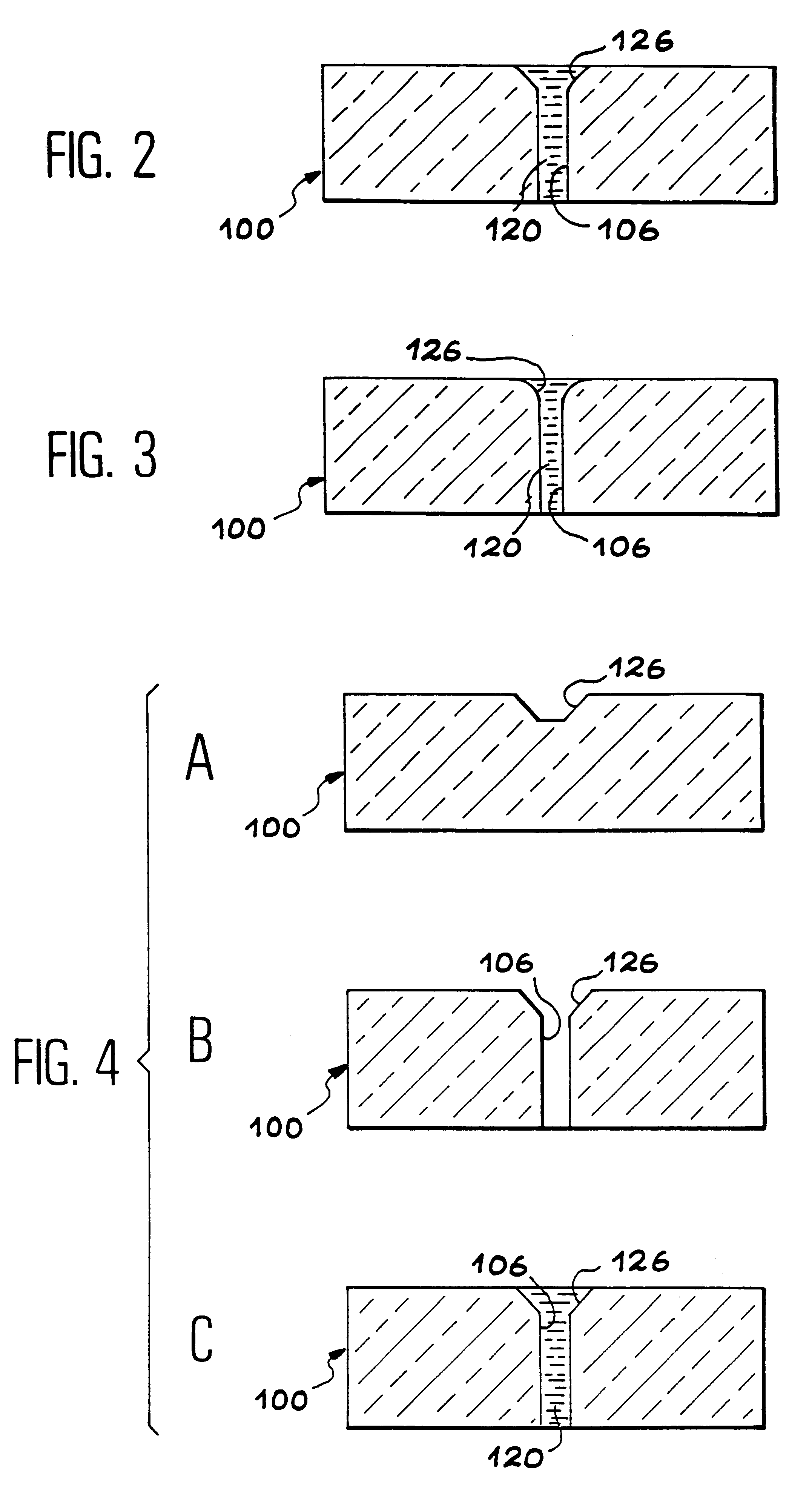
In order to achieve these purposes, the purpose of the invention is more specifically a process for physical isolation of regions of a substrate board comprising the following steps:

a) bonding of the substrate onto a support using ...


PUM

PropertyMeasurementUnit
thicknessaaaaaaaaaa
thicknessaaaaaaaaaa
physicalaaaaaaaaaa

Abstract

Process for physical isolation of regions (110) of a substrate board (100) comprising the following steps:a) formation of trenches (106) in the substrate, delimiting regions of the substrate (110),b) placement of a liquid bonding material (120) in the trenches, which can solidify and bond to the substrate board (100) when in the solid state,c) solidification of the bonding material.Application to isolation of electronic, optical, mechanical or magnetic components.

Description

TECHNICAL DOMAINThis invention relates to a process for preparation of a substrate board, and more precisely for the physical isolation of regions of a substrate board.For the purposes of the invention, physical isolation of regions means a separation between the various regions to electrically and / or optically and / or magnetically and / or mechanically (particularly piezoelectrically) isolate the said regions.The invention may be used in a very wide variety of applications in industry, depending on the isolation type planned.For example, a semiconductor substrate board with electrically isolated regions may be used to make electronic components, and particularly power switching components.In the same way, a substrate board comprising regions of transparent of double refraction material may be used for making wave guides, lenses or optical switches. Similarly, a substrate board comprising regions of piezoelectric or electro-optic materials may be used to make sensor or actuator matrice...

Claims


Application Information

Patent Timeline
Patent Type & Authority Patents(United States)
IPC IPC(8): H01L21/70H01L21/762H01L21/764H01L21/02H01L29/06
CPCH01L21/762H01L21/76224H01L21/764H01L24/96H01L29/0657H01L2924/01002H01L2924/01004H01L2924/01058H01L2924/01061H01L2924/01079H01L2924/01082H01L2924/01005H01L2924/01006H01L2924/01033H01L2924/01075
Inventor GIDON, PIERRE
Owner COMMISSARIAT A LENERGIE ATOMIQUE ET AUX ENERGIES ALTERNATIVES
Why Eureka
Try Eureka