Mounting structure of electronic component on substrate board

a technology of electronic components and mounting structures, applied in the direction of printed circuit aspects, electrical apparatus construction details, conductive pattern reinforcement, etc., can solve problems such as contact failur

Inactive Publication Date: 2001-10-16
DENSO CORP
View PDF7 Cites 34 Cited by
  • Summary
  • Abstract
  • Description
  • Claims
  • Application Information

AI Technical Summary

Problems solved by technology

Therefore, when the external shock is applied, the solder bump 102 may be detached from the portion A, resulting in a contact failure between the BGA package 101 and the multi-layer printed wiring board 103.

Method used


Image

  • Mounting structure of electronic component on substrate board
  • Mounting structure of electronic component on substrate board
  • Mounting structure of electronic component on substrate board

Examples


first embodiment

(First Embodiment)

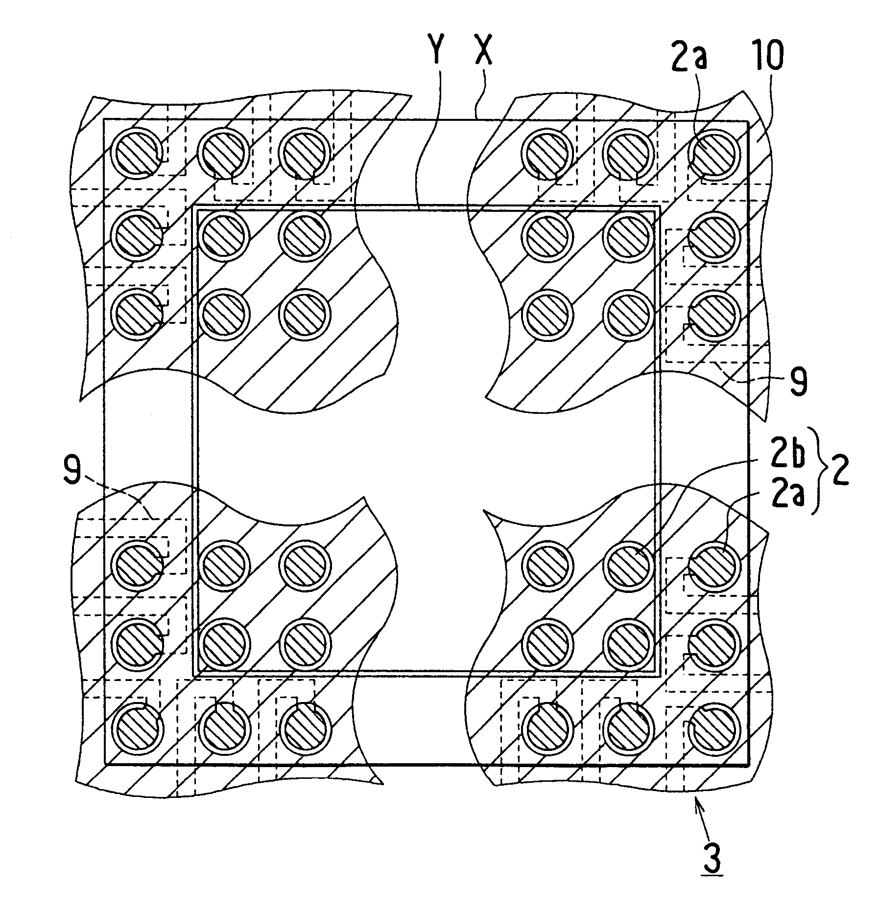
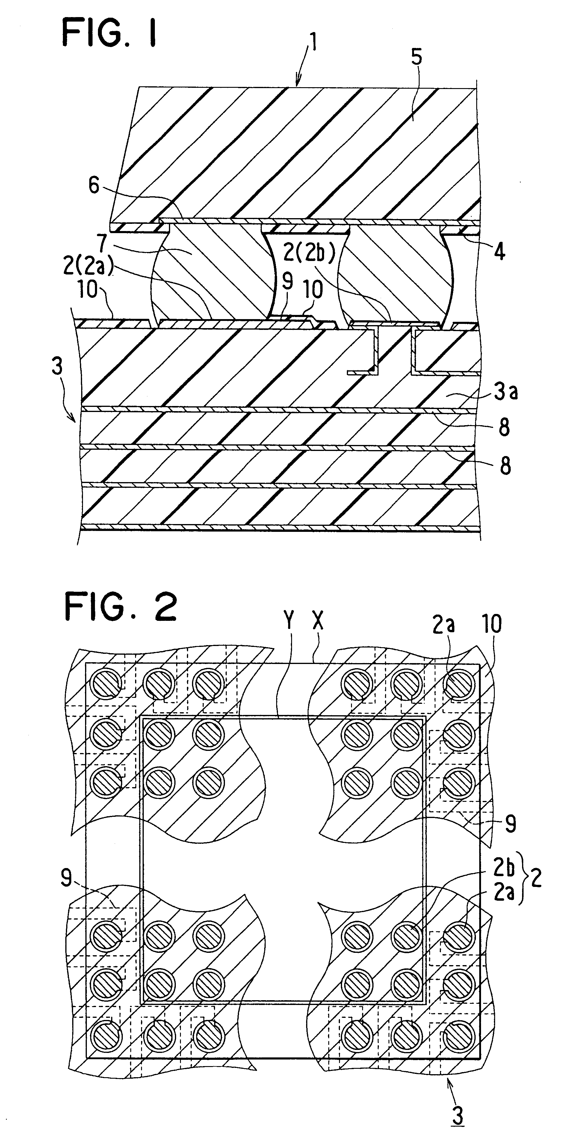
Referring to FIG. 1, a BGA package 1 is mounted on a multi-layer printed wiring board 3. The multi-layer printed wiring board 3 has a plurality of circular pad electrodes 2 arranged in a matrix form, as shown in FIG. 2. The multi-layer printed wiring board 3 can have any desired number of the electrodes 2 arranged in any desired pattern at any desired interval.

The method of forming the BGA package 1 will be described. A semiconductor chip (not shown) is attached to an interposer 4 having a circuit wiring layer 6 by adhesive, and is electrically connected to the circuit wiring layer 6 via gold (Au) wires or the like. Then, the semiconductor chip and the Au wires are integrally sealed by sealing resin 5. In the first embodiment, the interposer 4 is made of polyimide tape because polyimide tape can be readily thinned and produced at low cost, and the sealing resin 5 is made of epoxy resin, for example.

The interposer 4 constituting the back of the BGA package 1 has a p...

second embodiment

(Second Embodiment)

A second embodiment of the present invention will be described with reference to FIGS. 4, 5, 6A and 6B. In this and the following embodiments, description of components which are substantially the same to those in the previous embodiment is omitted.

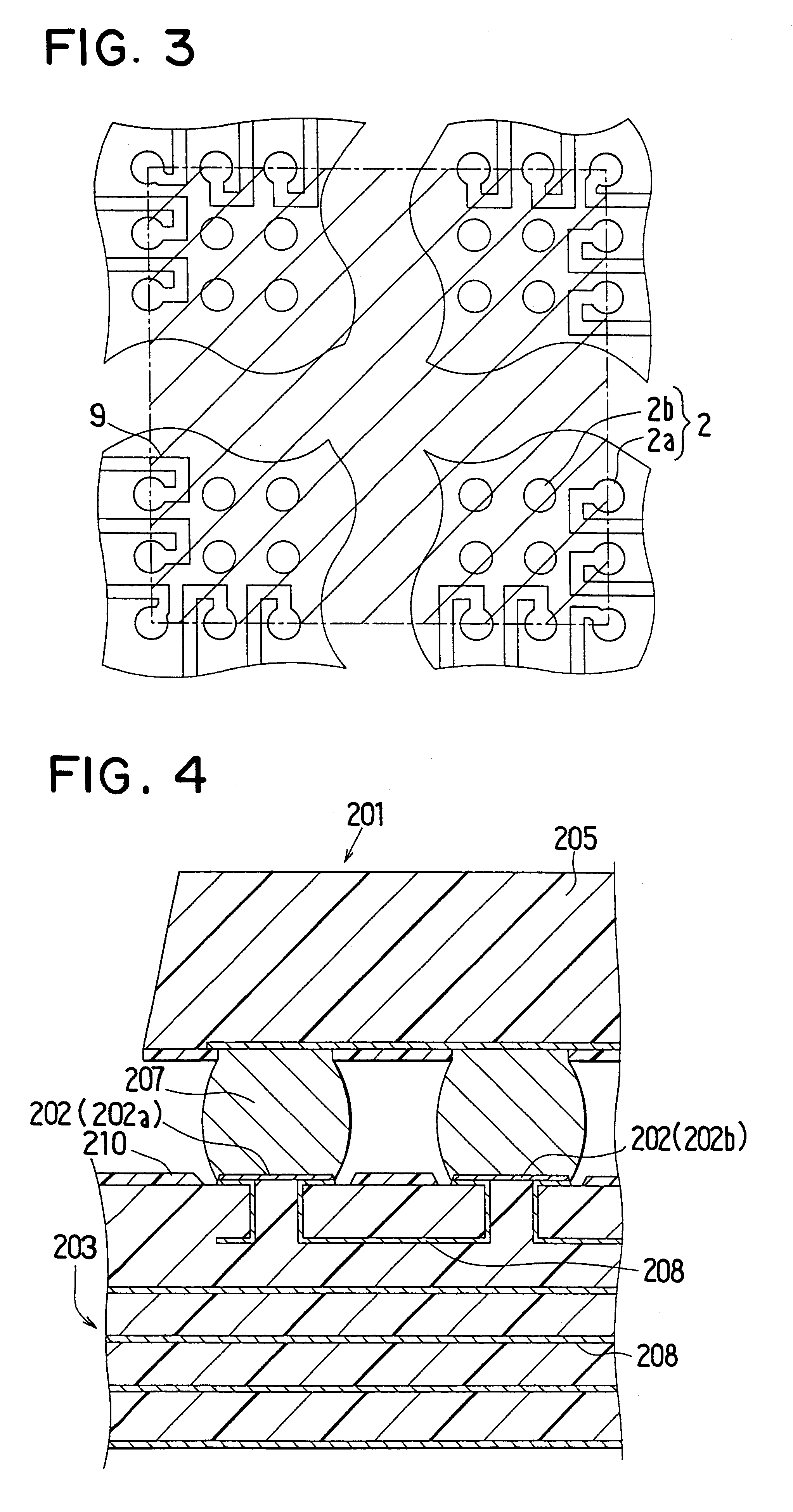
Referring to FIGS. 4, 5, in the second embodiment, lead wires from at least most-externally-located electrodes 202a (hereinafter referred to as external electrodes 202a), within an area X in FIG. 5, are not exposed on a multi-layer printed wiring board 203. On the other hand, some of inner electrodes 202b surrounded by the external electrodes 202a, within an area Y in FIG. 5, are provided with lead wires (not shown) exposed on the board 203.

In the second embodiment, in the same manner as in the first embodiment, pattern etching is performed on the surface of the multi-layer printed wiring board 203 so that lead wires are formed by the remaining copper foil, while parts of the copper foil to become electrodes 202 are lef...

third embodiment

(Third Embodiment)

A third embodiment of the present invention will be described with reference to FIG. 7.

In the second embodiment, wiring layers 208 embedded in a multi-layer printed wiring board 203 is used as a lead wire for the external electrode 202a. However, the embedded lead wire for the external electrode 202a may interfere with a lead wire extending from an inner electrode 202b located inside the external electrodes 202a if the embedded lead wire needs to be used for the inner electrode 202b. In the third embodiment, as shown in FIG. 7, some of the most-externally-located electrodes 302a (hereinafter referred to as external electrodes 302a) are provided with lead wires 309 extending on the surface layer of a multi-layer printed wiring board 303 in the same manner as in the first embodiment, and the rest of the external electrodes 302a are provided with the lead wires 309 made of the copper foil or the plated copper embedded in the board 303 in the same manner as in the seco...


PUM


Abstract

A BGA package is mounted on a multi-layer printed wiring board having a plurality of electrodes arranged in a matrix form through a plurality of solder bumps. In the most externally-located electrodes, a lead wire is formed to extend from a portion of the most-externally-located electrode located inside of a polygon formed by connecting each of the centers of adjacent most-externally-located electrodes. Therefore, the solder bumps are prevented from coming off the most-externally-located electrodes because a portion of the most-externally-located electrode to which stress caused by an external shock is intensively applied is located in an outside of the polygon. Thus, a contact failure between the BGA package and the multi-layer printed wiring board is prevented.

Description

This application relates to and claims priority from Japanese Patent Application Nos. Hei. 9-198829 filed on Jul. 24, 1997, 9-201751 filed on Jul. 28, 1997, 9-204729 filed on Jul. 30, 1997, 9-255568 filed on Sept. 19, 1997 and 9-255569 filed on Sep. 19, 1997, the contents of which are hereby incorporated by reference.1. Field of the InventionThe present invention relates to an electronic component mounted on a substrate board through an array of solder bumps attached to the back of the electronic component so that the electronic component is electrically connected to the substrate board, especially a mounting structure of the electronic component on the substrate board. The present invention is suitably applied to a mounting structure of an electronic component used in portable electronic equipments.2. Related ArtAs shown in FIG. 16, a conventional ball-grid array (hereinafter referred to as BGA) package 101 has an array of solder bumps 102 on its back surface, and a multi-layer pri...

Claims


Application Information

Patent Timeline
Patent Type & Authority Patents(United States)
IPC IPC(8): H01L23/498H01L23/48H05K3/24H05K1/11
CPCH01L23/49816H01L23/49838H05K1/112H05K3/244H01L2224/48227H01L2924/01039H01L2924/01046H01L2924/01078H01L2924/01079H01L2924/15311H05K2201/09227H05K2201/10734H01L24/48H01L2224/45144H01L2924/00H01L2224/32225H01L2224/48464H01L2224/73265H01L24/45H01L2224/45015H01L2924/12042H01L2924/181H01L2924/00014H01L2924/00012
Inventor KONDO, KENJIAOYAMA, MASAYUKIKONDO, KOJITAKEMOTO, MASANORIMIKURA, HIDEHIRONAKANO, TETUHIRO
Owner DENSO CORP
Why Eureka
Try Eureka