Wiring structure in a semiconductor device, method of forming the wiring structure, semiconductor device including the wiring structure and method of manufacturing the semiconductor device

a technology of semiconductor devices and wiring structures, which is applied in the direction of solid-state devices, contact members penetrating/cutting insulation/cable strands, basic electric elements, etc., can solve the problem of increasing the likelihood of contact holes being misaligned relative to conductive wiring or contact plugs, and becoming more difficult to form wirings by conventional manufacturing processes, etc. problem, to achieve the effect of improving electrical characteristics and improving electrical characteristics

Active Publication Date: 2008-01-03
LONGITUDE FLASH MEMORY SOLUTIONS LTD
View PDF6 Cites 23 Cited by
  • Summary
  • Abstract
  • Description
  • Claims
  • Application Information

AI Technical Summary

Benefits of technology

[0008]Example embodiments disclosed herein describe a wiring structure in a semiconductor device without a contact failure thereof. Example embodiments disclosed herein describe a method of forming a wiring structure in a semiconductor device without a contact failure by preventing chemicals from permeating therein. Example embodiments disclosed herein describe a semiconductor device including a wiring structure to ensure improved electrical characteristics. Example embodiments disclosed herein describe a method of manufacturing a semiconductor device including a wiring structure to ensure improved electrical characteristics.

Problems solved by technology

As the widths of wirings in conventional semiconductor devices become smaller, it becomes more difficult to form the wirings by conventional manufacturing processes.
Additionally, it may be difficult to form contact plugs that connect adjacent wirings at desired positions because contact plugs in conventional semiconductor device generally have a high aspect ratio.
As a result, the likelihood that the contact hole will be misaligned relative to the conductive wiring or contact plug increases.
If a misaligned contact hole exposes an undesired adjacent conductive wiring, the contact plug formed in the contact hole may cause a failure such as a bridge between adjacent conductive wirings.
However, the chemicals may permeate into an underlying contact plug or conductive wiring when the cleaning process or the etching process is carried out excessively.
As a result, the underlying contact plug or conductive wiring can become damaged.
When damaged, the underlying contact plug or conductive wiring may contribute to an electrical failure of the semiconductor device.
Generally, damage incurred by the underlying contact plug or conductive wiring increases as the alignment error of the contact plug increases.
For example, when the chemicals permeate into upper portions or lateral portions of the underlying contact plug or conductive wiring, conductive material in the contact plug or conductive wiring may become melted or eroded by the chemicals.
When the contact plug or the conductive wiring is partially melted or eroded by the chemicals, a contact resistance of the contact plug or conductive wiring can increase considerably or a contact failure of the contact plug or conductive wiring may occur.
Recently, it has been discovered that the contact plug may incur serious damage by the permeated chemicals since the contact plug generally includes reactive metal or metal silicide.

Method used


Image

  • Wiring structure in a semiconductor device, method of forming the wiring structure, semiconductor device including the wiring structure and method of manufacturing the semiconductor device
  • Wiring structure in a semiconductor device, method of forming the wiring structure, semiconductor device including the wiring structure and method of manufacturing the semiconductor device
  • Wiring structure in a semiconductor device, method of forming the wiring structure, semiconductor device including the wiring structure and method of manufacturing the semiconductor device

Examples


Embodiment Construction

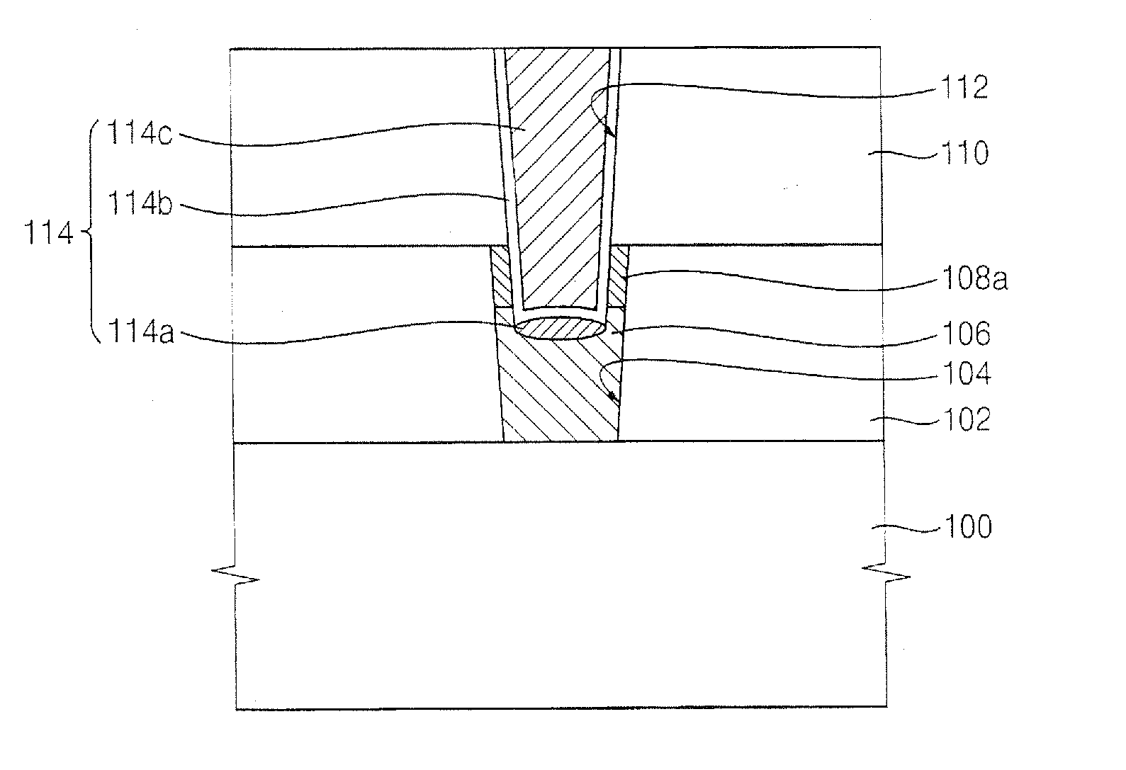
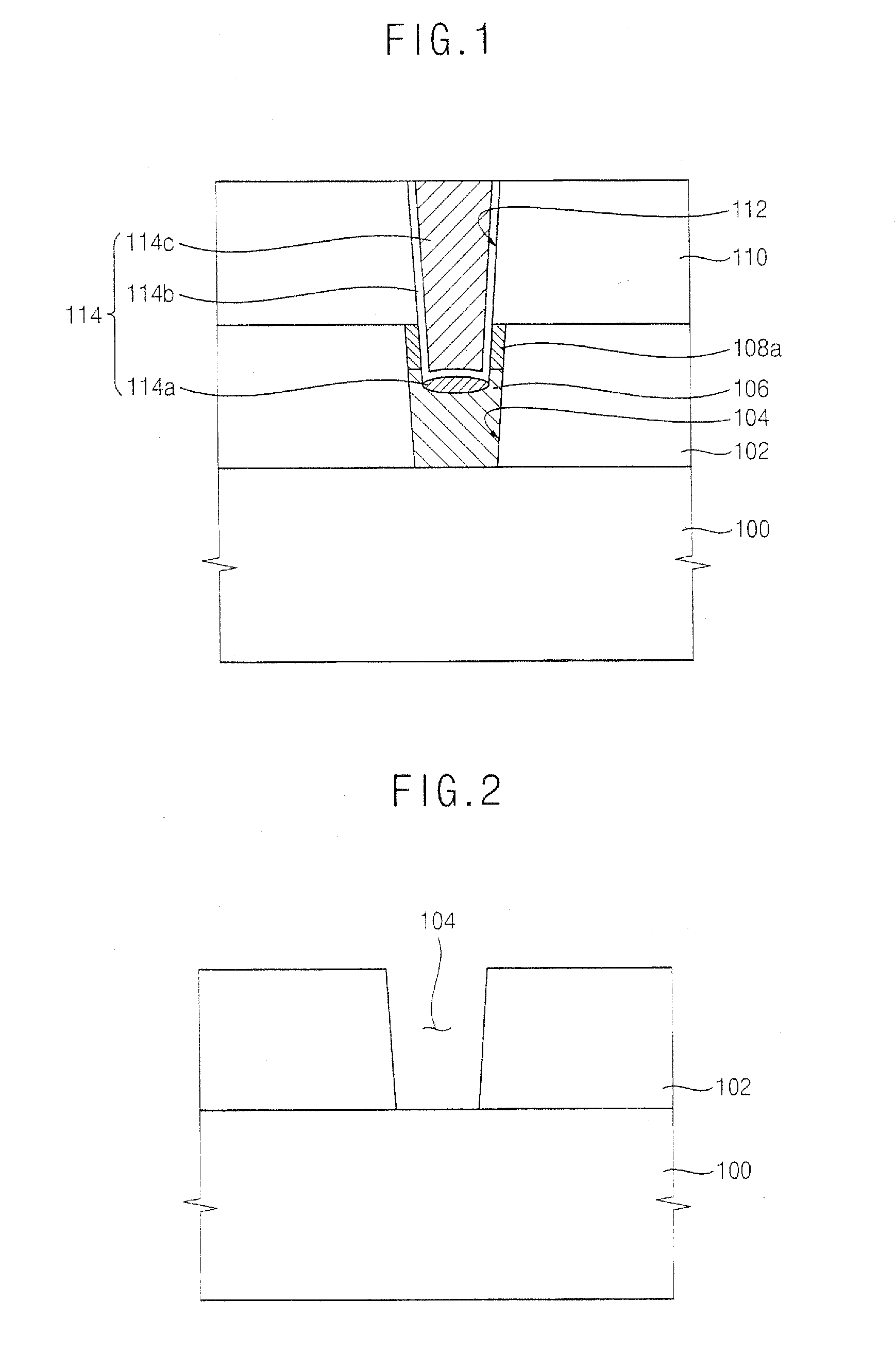
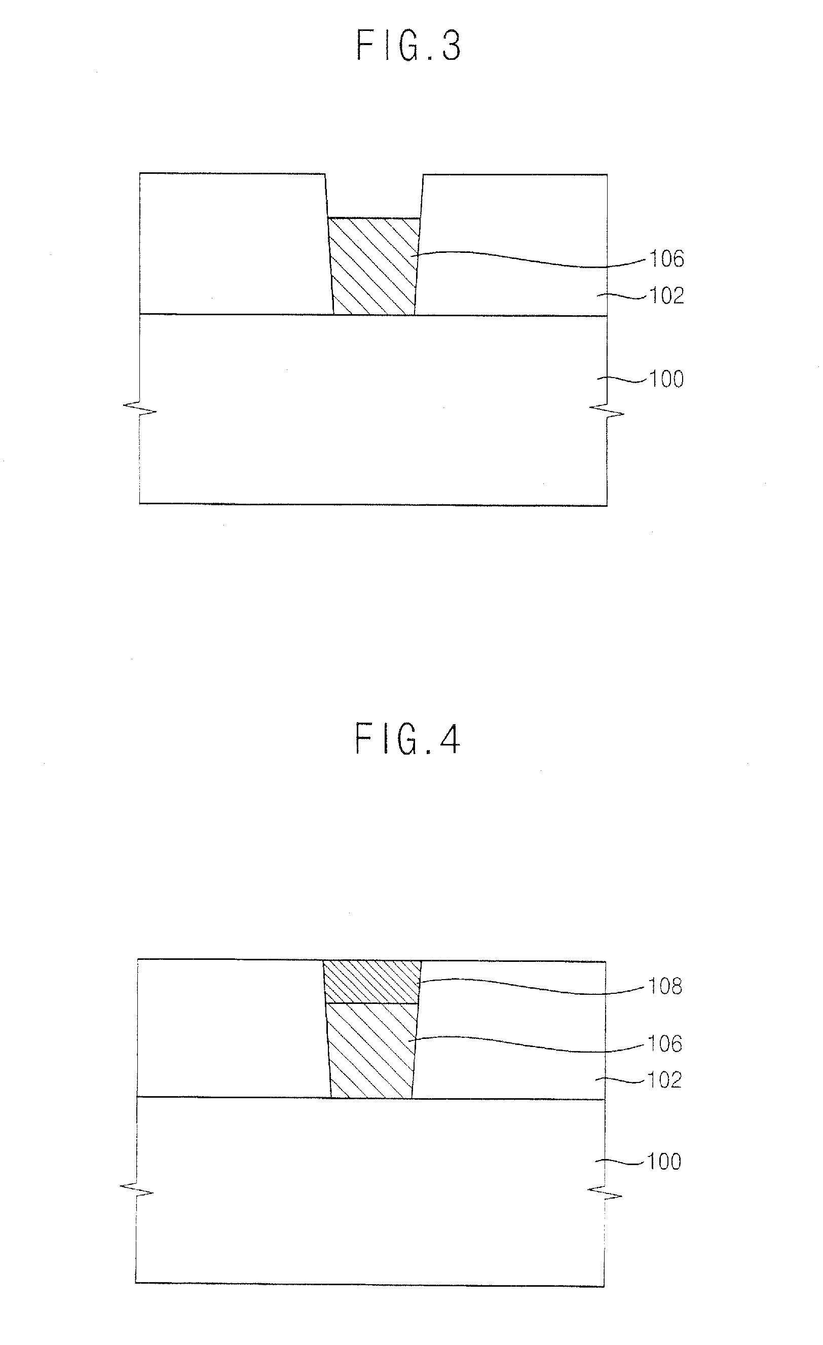
[0018]Example embodiments of the present invention will now be described more fully with reference to the accompanying drawings. These embodiments may, however, be realized in many different forms and should not be construed as limited to the example embodiments set forth herein. Rather, these example embodiments are provided so that this disclosure will be thorough and complete, and will fully convey the scope of the invention to those skilled in the art. In the drawings, the sizes and relative sizes of layers and regions may be exaggerated for clarity.

[0019]It will be understood that when an element or layer is referred to as being “on,”“connected to” or “coupled to” another element or layer, it can be directly on, connected or coupled to the other element or layer or intervening elements or layers may be present. In contrast, when an element is referred to as being “directly on,”“directly connected to” or “directly coupled to” another element or layer, there are no intervening el...


PUM


Abstract

A wiring structure in a semiconductor device may include a first insulation layer formed on a substrate, a first contact plug, a capping layer pattern, a second insulation layer and a second contact plug. The first insulation layer has a first opening that exposes a contact region of the substrate. The first contact plug is formed on the contact region to partially fill up the first opening. The capping layer pattern is formed on the first contact plug to fill up the first opening. The second insulation layer is formed on the capping layer pattern and the first insulation layer. The second insulation layer has a second opening passing through the capping layer pattern to expose the first contact plug. The second contact plug is formed on the first contact plug in the second opening. Since the wiring structure includes the capping layer pattern, the wiring structure may prevent a contact failure by preventing chemicals from permeating into the first contact plug.

Description

CROSS-REFERENCE TO RELATED APPLICATIONS[0001]This application claims the benefit of foreign priority under 35 USC § 119 to Korean Patent Application No. 2006-61792 filed on Jul. 3, 2006, the contents of which are herein incorporated by reference in their entirety.BACKGROUND[0002]1. Field of Invention[0003]Example embodiments of the present invention relate generally to wiring structures in semiconductor devices, methods of forming wiring structures, semiconductor devices including wiring structures, and methods of manufacturing semiconductor devices including wiring structures. More particularly, example embodiments of the present invention relate to a wiring structure in a semiconductor device capable of preventing a contact failure, a method of forming such a wiring structure, a semiconductor device including such a wiring structure, and a method of manufacturing a semiconductor device including such a wiring structure.[0004]2. Description of the Related Art[0005]As electronic dev...

Claims


Application Information

Patent Timeline
Patent Type & Authority Applications(United States)
IPC IPC(8): H01R4/24
CPCH01L21/76805H01L21/76834H01L21/76855H01L23/5226H01L27/10855H01L27/10888H01L21/76889H01L2924/0002H01L21/76831H10B12/0335H10B12/485H01L2924/00H01L21/28
Inventor BAE, KI-SOONCHOI, SEI-RYUNG
Owner LONGITUDE FLASH MEMORY SOLUTIONS LTD
Why Eureka
Try Eureka