
Electroplating process for preparing a Ni layer of biaxial texture

a technology of ni-plated layer and biaxial texture, which is applied in the field of ni-plated layer with biaxial texture, can solve the problems of uni-axial texture limitation, and inability to prepare a plated layer of biaxial textur

Inactive Publication Date: 2002-02-12
KOREA INST OF MASCH & MATERIALS
View PDF6 Cites 53 Cited by
  • Summary
  • Abstract
  • Description
  • Claims
  • Application Information

AI Technical Summary

Problems solved by technology

Thus, it has been regarded as impossible to prepare a plated layer of biaxial texture in which crystal orientation is arranged uniformed in the direction of the c-axis as well as the a-axis and the b-axis.
No research has been conducted on the preparation of plated layers which are of biaxial texture.
However, this is also confined to uni-axial textures.
However, such a large current generates heat which may be of large enough energy to burn the coils.
Hence, to generate a magnetic field at an intensity of more than 1 T is unfavorable in terms of economy and practice.
For example, if the thermal treatment is conducted at lower than 400.degree. C., the driving force for the diffusion of atoms is too small to cause a change in the texture of the plated layer.
Or, the atoms diffuse at too low speeds to gain economical profits.
On the other hand, at more than 1,400.degree. C., the Ni plated layer suffers from being seriously softened, so its mechanical strength becomes poor to the extent that it cannot sustain its own weight.
Thus, to carry out the thermal treatment at more than 1,400.degree. C. is practically useless.

Method used


Image

  • Electroplating process for preparing a Ni layer of biaxial texture
  • Electroplating process for preparing a Ni layer of biaxial texture
  • Electroplating process for preparing a Ni layer of biaxial texture

Examples


Embodiment Construction

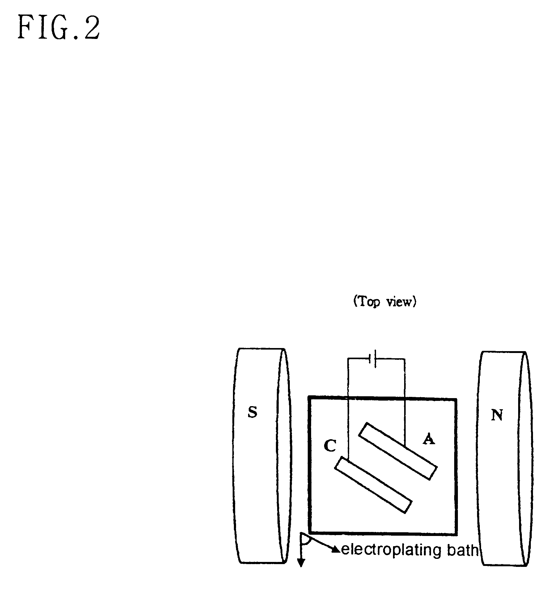
Using the electroplating process described above, Ni-plated layers were formed on various substrates under the conditions indicated in Table 2 and then, subjected to heat treatment according to the indications of Table 2, below. The Ni-plated layers, which thus had biaxial textures, were analyzed and the results are given in Table 2.

As apparent from the data of Table 2, all of the samples tested were 0.96 or greater in TF and their FWHMs were 6.37.degree. or smaller in terms of .theta.-rocking curve and 21.degree. or smaller in terms of .phi.-scan. Therefore, the Ni-plated layer prepared according to the present invention is of excellent biaxial texture.

As described hereinbefore, the present invention provides an electroplating process by which a Ni-plated layer of biaxial texture can be formed on various substrates. Thus, the present invention allows YBCO superconducting cables to be used as substrates for which vacuum deposition can be applied. In addition, the electroplating proc...


PUM

PropertyMeasurementUnit
Timeaaaaaaaaaa
Angleaaaaaaaaaa
Angleaaaaaaaaaa

Abstract

Disclosed is an Ni-plated layer of biaxial texture, which is formed by electroplating. In the Ni-plated layer,peaks measured on a theta-rocking curve have a FWHM of 7° or less in terms of the misorientation on the c-axis; and peaks measured on phi-scan have a FWHM of 21° or less in terms of the misorientation on the plane formed by the a-axis and the b-axis. Also, a process of electroplating a Ni layer are disclosed. The process comprises forming a Ni-plated layer of biaxial texture under a magnetic field by electroplating and subjecting the Ni-plated layer to thermal treatment to develop the biaxial texture. This electroplating process is expected to give a significant contribution to the development of the electroplating technology and to replace the vacuum deposition used for the preparation of thin film magnetic materials or thin film piezoelectric materials.

Description

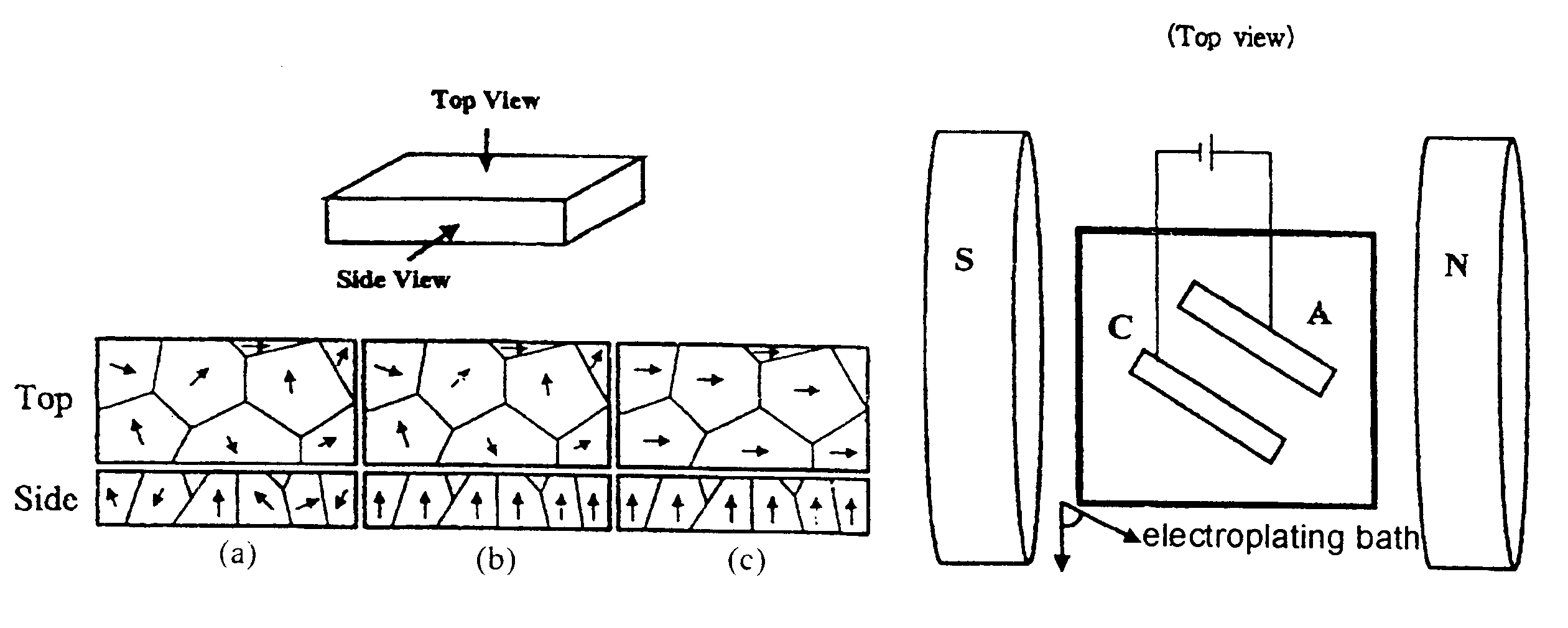
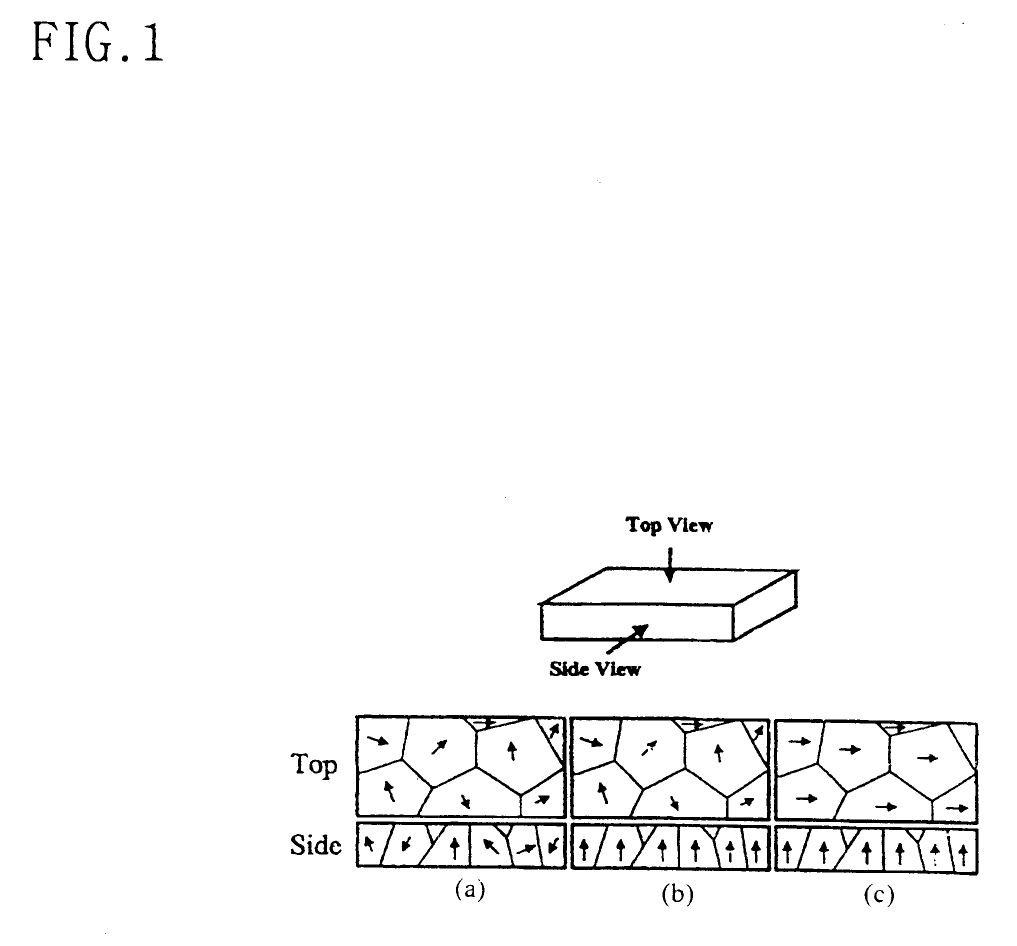
1. Field of the InventionThe present invention relates to a Ni-plated layer with a biaxial texture, which is excellent in toughness and magnetic properties and useful as substrate for coating YBCO Super conductor cable. Also, the present invention is concerned with an electroplating process of and an apparatus for preparing the Ni-plated layer.2. Description of the Prior ArtIn a polycrystalline material, a texture refers to a single cluster structure consisting of a number of crystal particles which have the same crystal orientation in a polycrystalline material. The texture is generally divided into two groups: fiber texture and three-dimensional texture.In order to better understand the background of the invention, a description will be given of the texture in conjunction with FIG. 1.FIG. 1 schematically shows textures in board planks. FIG. 1a is a schematic view showing the absence of textures. Shown in FIG. 1b is a uni-axial texture, generically designated "fiber texture". The f...

Claims


Application Information

Patent Timeline
IPC IPC(8): C25D5/18C25D5/00C25D3/12
CPCC25D3/12C25D5/006C25D5/50C25D5/18C25D5/009C25D5/617
Inventor LEE, KYU HWANCHUNG, HYUNG-SIKLEE, SANG ROCHANG, DOYONJEONG, YONGSOOYOO, JAIMOOKO, JAE-WOONGKIM, HAI-DOO
Owner KOREA INST OF MASCH & MATERIALS
Learn More