Piezoelectric thin film element and piezoelectric thin film device

a thin film element and piezoelectric technology, applied in the direction of device material selection, vacuum evaporation coating, generator/motor, etc., can solve the problems of remarkable variation or deterioration of properties, reduced insulating performance of knn thin film, and piezoelectric properties, and achieve small leak current and small deterioration of piezoelectric constant

Active Publication Date: 2011-07-21
SUMITOMO CHEM CO LTD
View PDF9 Cites 14 Cited by
  • Summary
  • Abstract
  • Description
  • Claims
  • Application Information

AI Technical Summary

Benefits of technology

[0010]An object of the present invention is to provide a piezoelectric thin film element having a small leak current, and having a smal

Problems solved by technology

However, in a piezoelectric material fabricated by a sintering method, being a conventional method, as a thickness thereof becomes smaller, particularly as the thickness becomes nearly about 10 μm, a thickness of the piezoelectric thin film corresponds to almost a size of each crystal grain constituting the thin film, and an influence on the piezoelectric properties, etc, can not be ignored.
Therefore, there is a problem that variation or deterioration of properties is remarkable.
However, in a

Method used


Image

  • Piezoelectric thin film element and piezoelectric thin film device
  • Piezoelectric thin film element and piezoelectric thin film device
  • Piezoelectric thin film element and piezoelectric thin film device

Examples


examples

[0061]Next, examples of the present invention will be described.

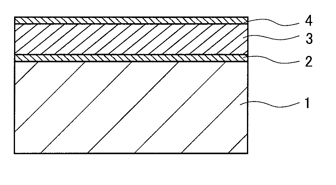
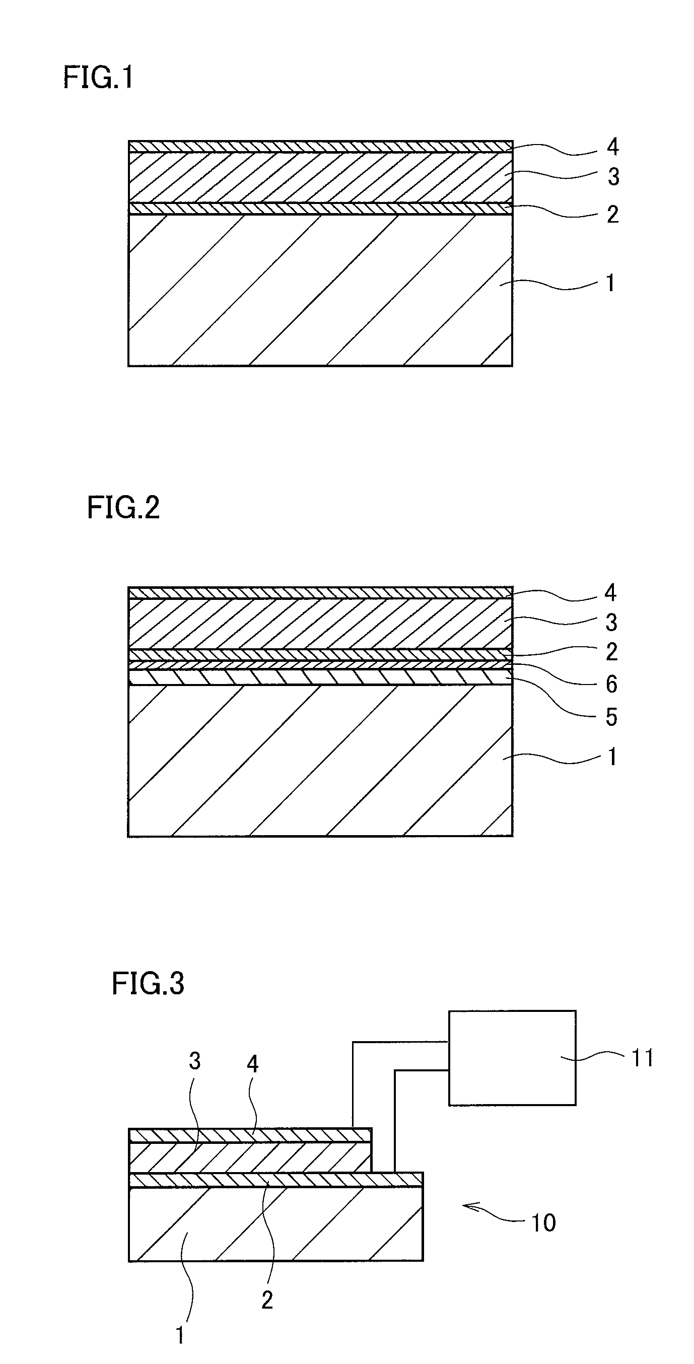
[0062]The piezoelectric thin film element of examples 1 to 20 and comparative examples 1 to 14 has a cross-sectional structure similar to the embodiment shown in FIG. 2, and Ti adhesive layer, Pt lower electrode, KNN piezoelectric thin film, and Pt upper electrode are laminated on the Si substrate having a thermal oxide film.

[Film Deposition of the KNN Thin Film]

[0063]A film deposition method of the KNN piezoelectric thin film according to examples and comparative examples will be described hereafter.

[0064]Si substrate with thermal oxide film was used as the substrate ((100) plane orientation, thickness: 0.525 mm, size: 20 mm×20 mm, thickness of the thermal oxide film: 200 nm). First, Ti adhesive layer (film thickness: 2 nm) and Pt lower electrode ((111) plane preferential orientation, film thickness: 200 nm) were formed on the substrate by RF magnetron sputtering. The Ti adhesive layer and the Pt lower electrode were f...


PUM

PropertyMeasurementUnit
Angleaaaaaaaaaa
Angleaaaaaaaaaa
Fractionaaaaaaaaaa

Abstract

To provide a piezoelectric thin film on a substrate, having an alkali-niobium oxide-based perovskite structure expressed by a composition formula (K1−xNax)yNbO3, wherein the composition ratio x of the piezoelectric thin film expressed by (K1−xNax)yNbO3 is in a range of 0.4≦x≦0.7, and a half width of a rocking curve of (001) plane by X-ray diffraction measurement is in a range of 0.5° or more and 2.5° or less.

Description

[0001]The present application is based on Japanese Patent Application No.2010-007942, filed on Jan. 18, 2010, the entire contents of which are hereby incorporated by reference.BACKGROUND OF THE INVENTION[0002]1. Field of the Invention[0003]The present invention relates to a piezoelectric thin film element and a piezoelectric thin film device, using a piezoelectric thin film of alkali-niobium oxide series.[0004]2. Description of the Related Art[0005]A piezoelectric ceramics is processed into various piezoelectric elements in accordance with various purposes, and is widely used particularly as a functional electronic component such as an actuator for generating deformation by adding a voltage to the piezoelectric elements, and a sensor for detecting the voltage generated by deformation of the piezoelectric elements. As the piezoelectric ceramics used for the purpose of use of the actuator and the sensor, a dielectric material, being a lead-based material, having excellent piezoelectri...

Claims


Application Information

Patent Timeline
IPC IPC(8): H01L41/08H01L41/18H01L41/047C04B35/00C23C14/06H01L41/09H01L41/187H01L41/22H01L41/29H01L41/316H01L41/39
CPCH01L41/18H01L41/094H03H9/02031H10N30/2042H10N30/8542H10N30/076
Inventor SHIBATA, KENJISUENAGA, KAZUFUMINOMOTO, AKIRAWATANABE, KAZUTOSHI
Owner SUMITOMO CHEM CO LTD
Why Eureka
Try Eureka