
Seed selection and growth methods for reduced-crack group iii nitride bulk crystals

a nitride and bulk crystal technology, applied in the field of bulk crystals, can solve the problems of difficult to grow gan crystal ingots, impede the realization of high-end optical and electronic devices, and high cost of gan substrates

Active Publication Date: 2016-07-28
SIXPOINT MATERIALS
View PDF2 Cites 13 Cited by
  • Summary
  • Abstract
  • Description
  • Claims
  • Application Information

AI Technical Summary

Benefits of technology

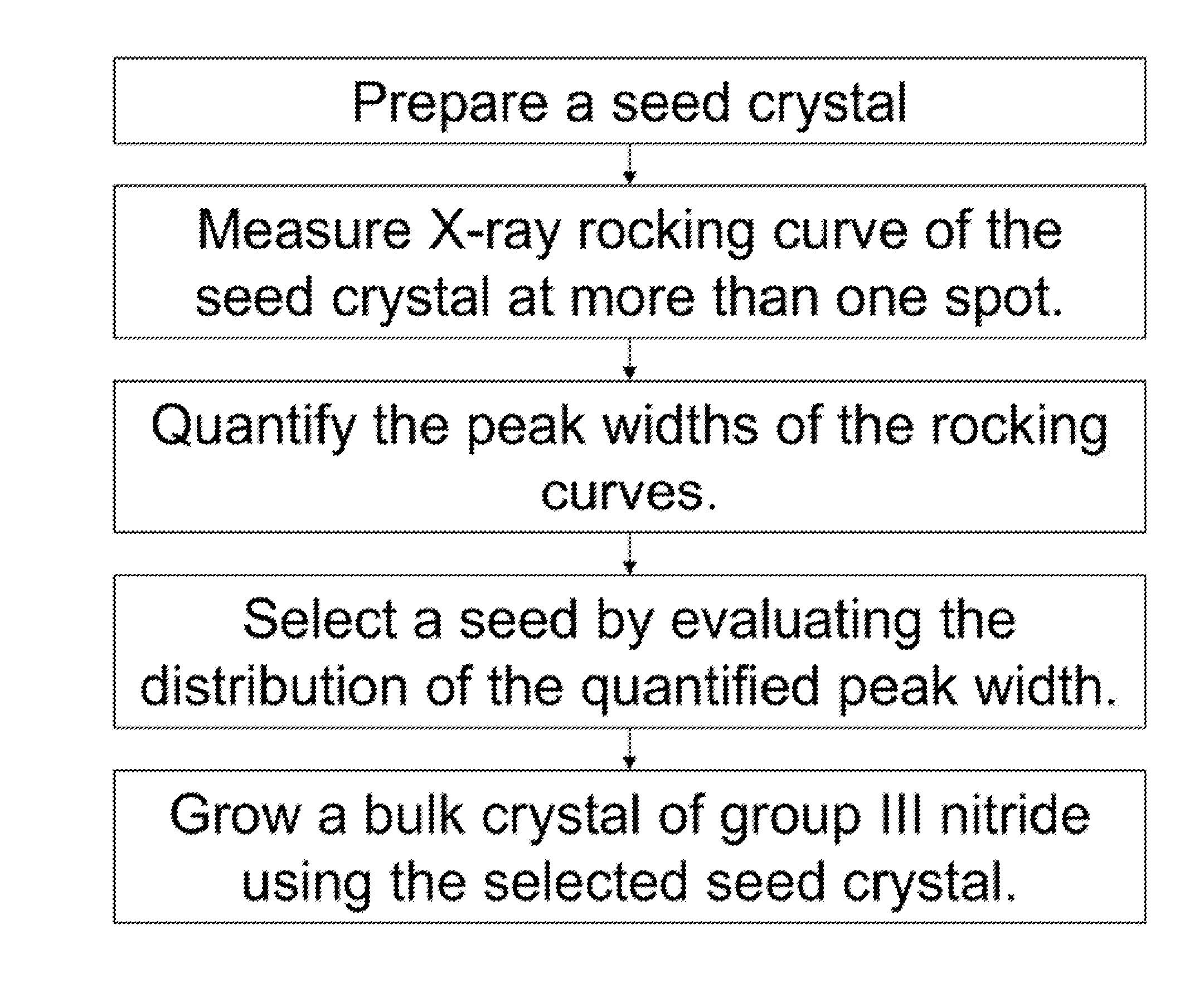
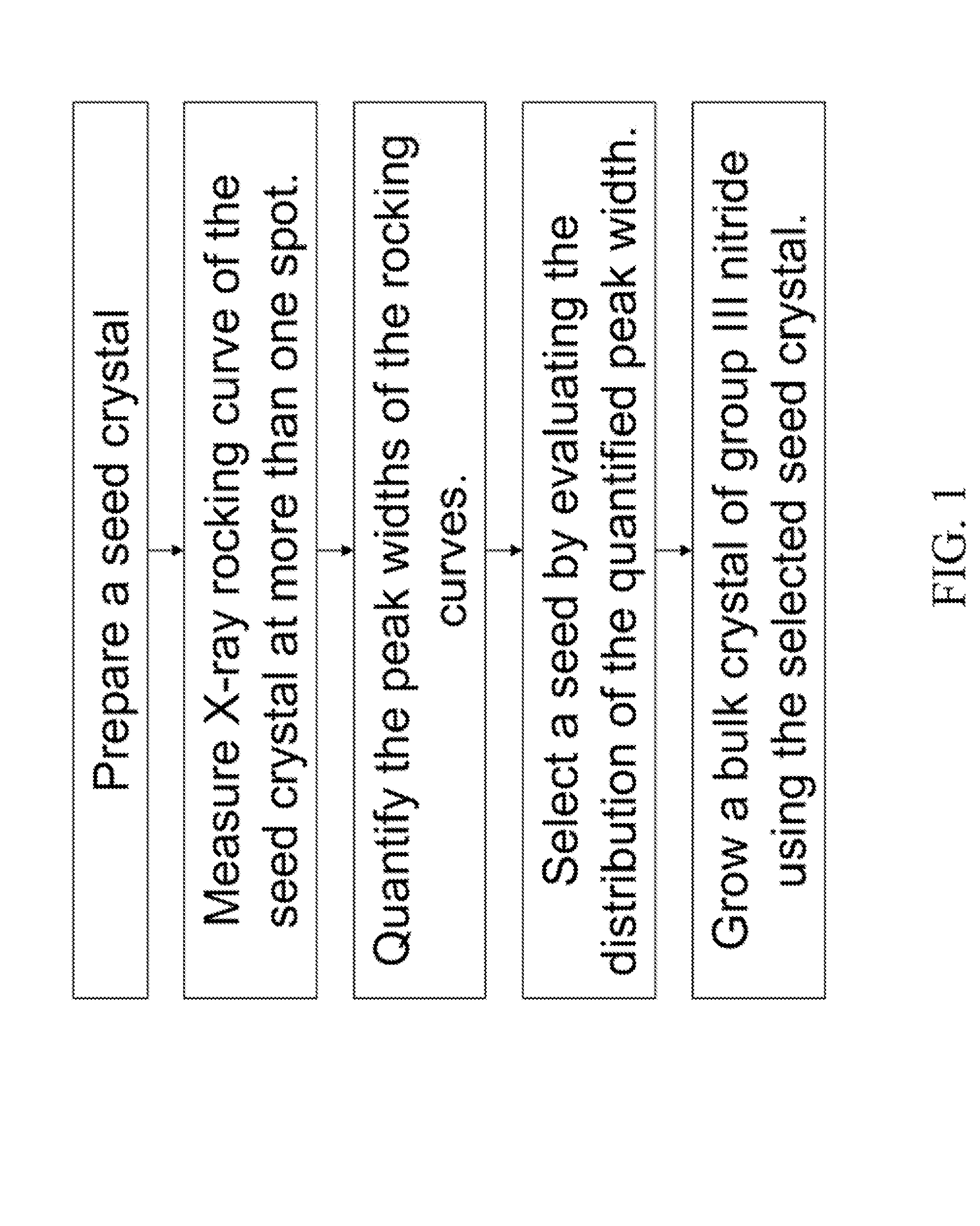
The invention provides a method for growing bulk crystals of group III nitride using a seed crystal that is selected based on its x-ray rocking curves. The method includes measuring the x-ray rocking curves at multiple points, quantifying the peak widths, and analyzing the distribution of the peak widths. This method allows for the selection of an efficient seed crystal for growing group III nitride crystals.

Problems solved by technology

However, the majority of these devices are grown epitaxially on heterogeneous substrates, such as sapphire and silicon carbide because GaN substrates are extremely expensive compared to these heteroepitaxial substrates.
The heteroepitaxial growth of group III nitride causes highly defected or even cracked films, which hinder the realization of high-end optical and electronic devices, such as high-brightness LEDs for general lighting or high-power microwave transistors.
However, due to the high melting point and high nitrogen vapor pressure at elevated temperature, it has been difficult to grow GaN crystal ingots.
HVPE is one of vapor phase methods, which has difficulty in reducing dislocation density less than 105 cm−2.
However, we found it quite challenging to avoid cracking of bulk crystals, especially when the total thickness of the bulk crystal exceeds 1 mm.
We believe that the cracking problem in bulk group III nitride is a universal problem for any bulk growth methods including the ammonothermal method.
Due to limited availability and high cost of single crystalline substrates of group III nitride, these devices have been fabricated on so-called heteroepitaxial substrates such as sapphire and silicon carbide.
Currently, the majority of commercially available GaN substrates is produced with HVPE, in which it is difficult to reduce the dislocation density to less than 105 cm−2.
However, it is challenging to obtain a bulk crystal over 1 mm thick without cracking.
Nevertheless, we have experienced cracking problem even with such selection procedure.
Although the origin and mechanism for crack formation are not well known, a possible cause would be stress accumulation inside the crystal due to a slight mismatch of thermal expansion coefficient or other physical properties between the seed crystal and grown crystal.

Method used


Image

  • Seed selection and growth methods for reduced-crack group iii nitride bulk crystals
  • Seed selection and growth methods for reduced-crack group iii nitride bulk crystals
  • Seed selection and growth methods for reduced-crack group iii nitride bulk crystals

Examples


example 1

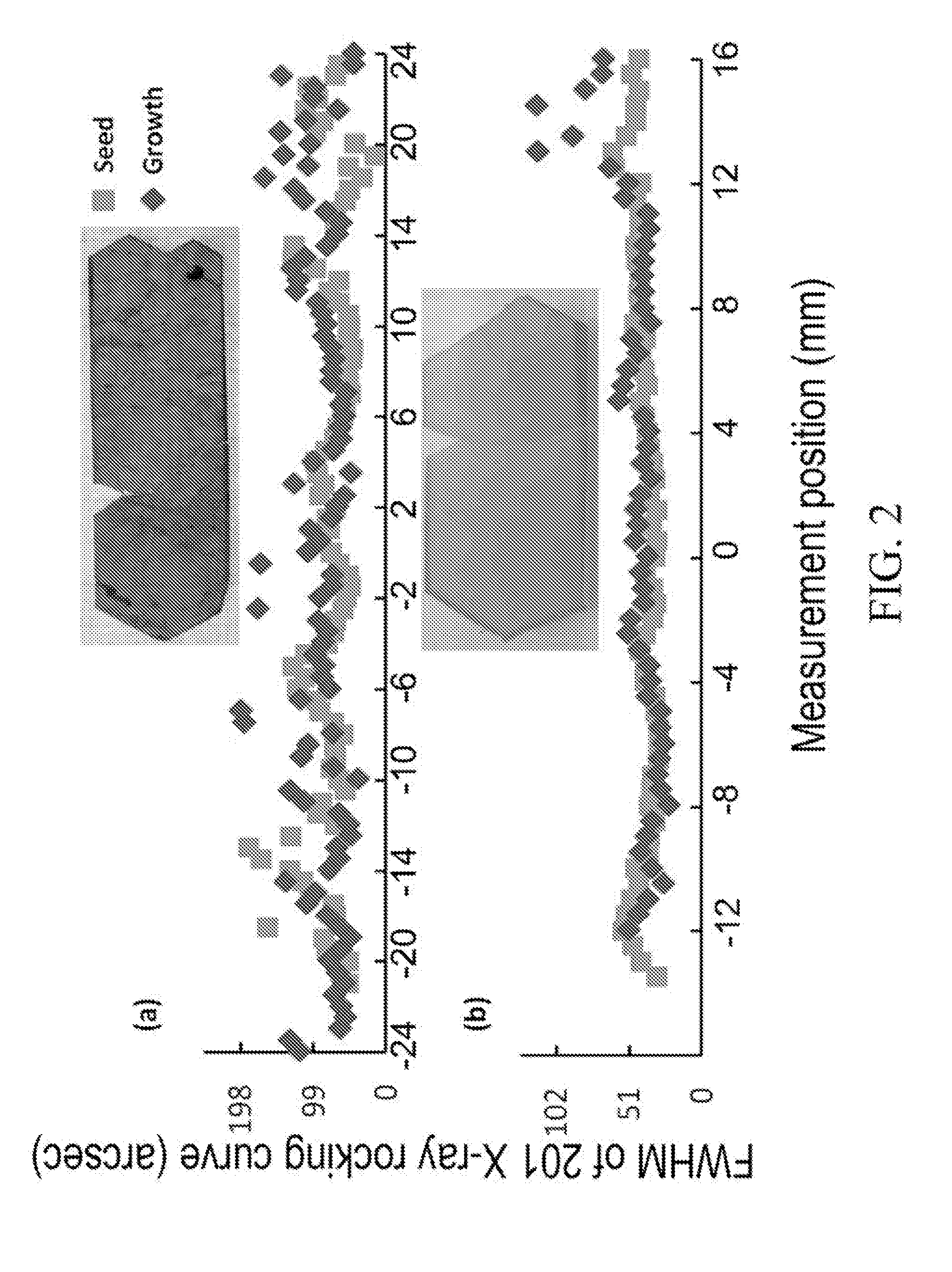
[0048]Single crystalline GaN seed crystal having a basal plane of c-plane was prepared with HVPE. The thickness of the GaN seed was approximately 430 microns. X-ray rocking curves from 201 reflection were recorded from multiple spots of the nitrogen polar side of the seed crystal. The measurement was conducted along the m-direction with the spot separation of 0.5 mm. The peak width is quantified with FWHM in arcsec. The square dots in FIG. 2 (a) show FWHM at each measurement spot. As shown in the FIG. 2(a) the FWHM values have a large scattering. The mean value of the FWHM was 78 arcsec and the standard deviation was 29 arcsec, which was 37% of the mean value. The data scattering is seen throughout the scanned line.

[0049]Then, a bulk crystal of GaN was grown in supercritical ammonia using a high-pressure reactor. The chamber within the high-pressure reactor was divided into a lower part and an upper part with baffle plates. Approximately 15 g of polycrystalline GaN is used as a nutr...

example 2

[0051]Similar to Example 1, a c-plane GaN seed crystal was prepared with HVPE. The thickness of the GaN seed was approximately 430 microns. X-ray rocking curves from 201 reflection were recorded from multiple spots of the nitrogen polar side of the seed crystal. The measurement was conducted along a m-direction with spot separation of 0.5 mm. The peak width is quantified with FWHM in arcsec. The square dots in FIG. 2 (b) show FWHM at each measurement spot. As shown in the FIG. 2(b) the FWHM values have a small scattering. The mean value of the FWHM was 41 arcsec and the standard deviation was 7 arcsec, which was 17% of the mean value.

[0052]Then bulk GaN was grown on this seed crystal in a similar way as in Example 1. The FWHMs of 201 X-ray rocking curves from multiple spots on the grown bulk crystal are plotted with diamond dots in FIG. 2(b), showing small data scattering. The mean value of the FWHM was 48 arcsec and the standard deviation was 18 arcsec, which was 38% of the mean va...


PUM


Abstract

In one instance, the invention provides a method of growing bulk crystal of group III nitride using a seed crystal selected by (a) measuring x-ray rocking curves of a seed crystal at more than one point, (b) quantifying the peak widths of the measured x-ray rocking curves, and (c) evaluating the distribution of the quantified peak widths. The invention also includes the method of selecting a seed crystal for growing bulk crystal of group III nitride.The bulk crystal of group III nitride can be grown in supercritical ammonia or a melt of group III metal using at least one seed selected by the method above.

Description

CROSS REFERENCE TO RELATED APPLICATIONS[0001]This application claims benefit of priority to U.S. application Ser. No. 62 / 106,709 filed Jan. 22, 2015, entitled “Seed Selection and Growth Methods for Reduced-Crack Group III Nitride Bulk Crystals,” inventors Tadao Hashimoto, Edward Letts, and Daryl Key, attorney docket no. SIXPOI-024USPRV1, and this application is also related to the following:[0002]PCT Utility Patent Application Serial No. US2005 / 024239, filed on Jul. 8, 2005, by Kenji Fujito, Tadao Hashimoto and Shuji Nakamura, entitled “METHOD FOR GROWING GROUP III-NITRIDE CRYSTALS IN SUPERCRITICAL AMMONIA USING AN AUTOCLAVE,” attorneys' docket number 30794.0129-WO-01 (2005-339-1);[0003]U.S. Utility patent application Ser. No. 11 / 784,339, filed on Apr. 6, 2007, by Tadao Hashimoto, Makoto Saito, and Shuji Nakamura, entitled “METHOD FOR GROWING LARGE SURFACE AREA GALLIUM NITRIDE CRYSTALS IN SUPERCRITICAL AMMONIA AND LARGE SURFACE AREA GALLIUM NITRIDE CRYSTALS,” attorneys docket number...

Claims


Application Information

Patent Timeline
IPC IPC(8): C30B7/10G01N23/207C30B29/40
CPCC30B7/105C30B29/406G01N2223/056G01N2223/1016G01N23/207G01N2223/602
Inventor HASHIMOTO, TADAOLETTS, EDWARDKEY, DARYL
Owner SIXPOINT MATERIALS
Learn More