

Nitride semiconductor substrate, production method therefor and nitride semiconductor device
a technology of nitride semiconductor and production method, which is applied in the direction of polycrystalline material growth, crystal growth process, chemically reactive gas, etc., can solve the problems of difficult cmp of nitride semiconductor crystals such as gan, poor surface quality, and many room left for improvement in their properties, etc., to inhibit variation in crystalline orientation, excellent in crystalline quality, excellent quality
- Summary
- Abstract
- Description
- Claims
- Application Information
AI Technical Summary
Benefits of technology
Problems solved by technology
Method used
Image

Examples
example 1
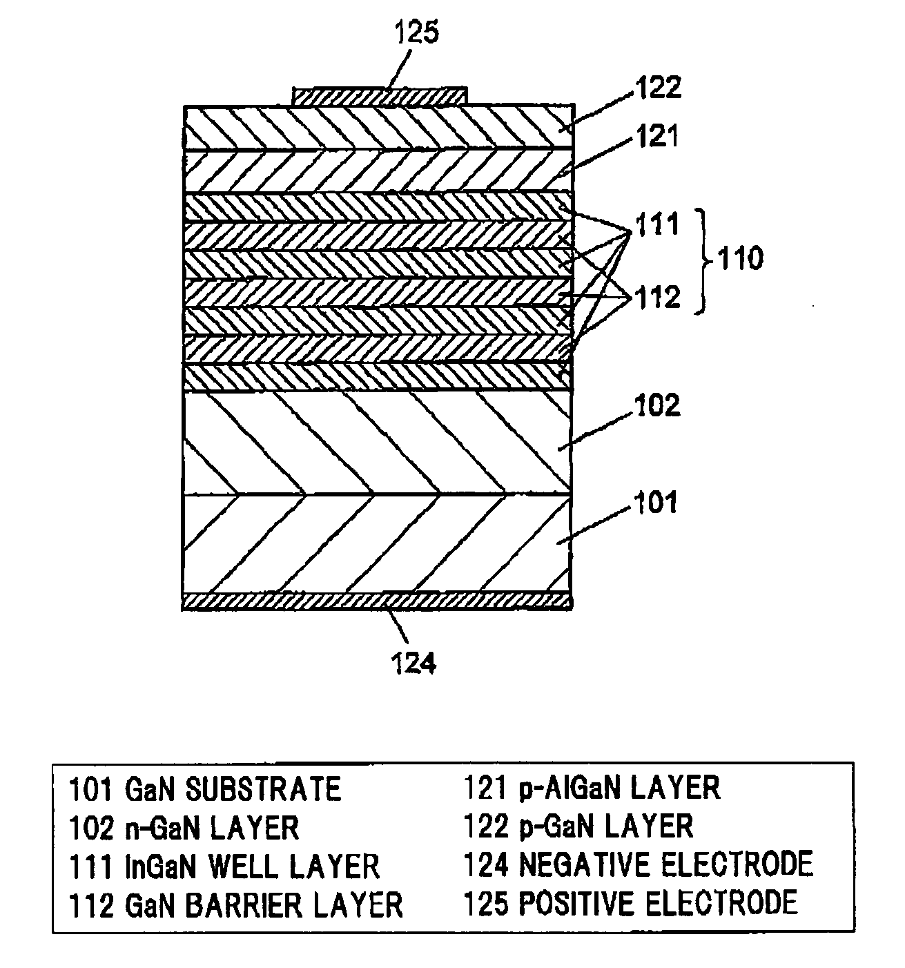
C-Plane GaN
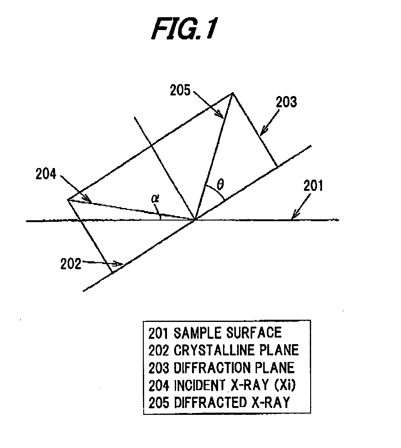
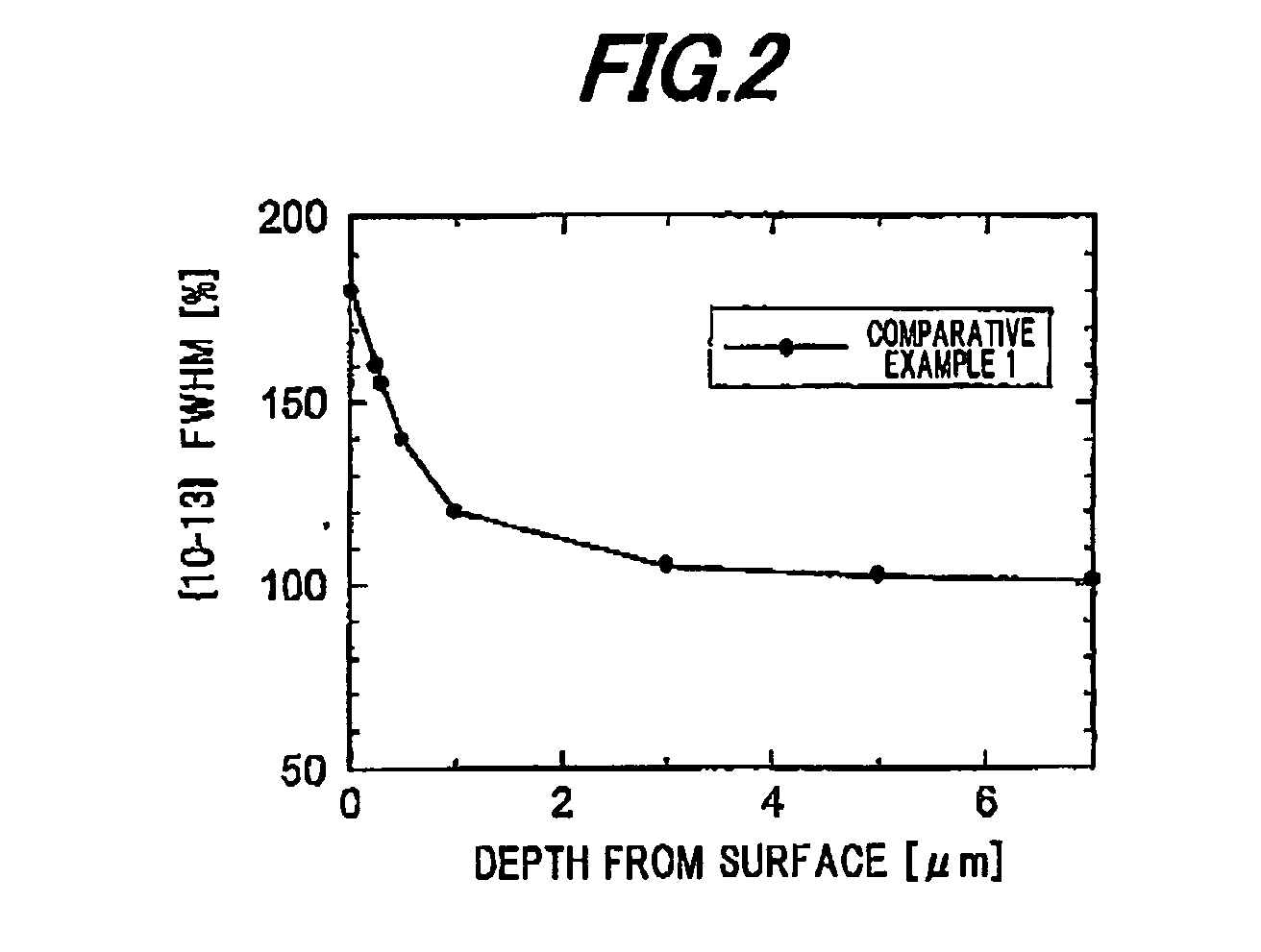
[0067]Comparative example 2 is followed by the below-described steps of processing this substrate surface. First is prepared a 1 mol % ammonium fluoride solution with gallium oxide nanopowder (average particle diameter: less than 50 nm) dispersed thereinto. Subsequently, the substrate is attached to a polishing shaft. Using a Teflon (registered trademark) polishing pad, and rotating the substrate at 20 rpm and a surface plate (Ø 400 mm) at 80 rpm, the substrate is polished. Dripping the prepared solution as needed, the polished substrate is irradiated with xenon lamp ultraviolet rays (irradiation intensity: 100 mW / cm2) for approximately 3 hours. The processing is again followed by the X-ray evaluation in the same manner as in Comparative examples 1 and 2. Its results are shown in FIG. 3, together with the results of Comparative example 2. The results are normalized to take the FWHM at a sufficiently inner portion of the crystal to be 100%. The {10-13} FWHM is as substanti...
example 2
M-Plane GaN
[0069]Comparative example 3 is followed by the below-described steps of processing this substrate surface. First is prepared a 0.5 mol % ammonium fluoride solution with gallium oxide nanopowder (average particle diameter: less than 50 nm) dispersed thereinto. Subsequently, the substrate is attached to a polishing shaft. Using a polyurethane polishing pad, and rotating the substrate at 20 rpm and a surface plate (Ø 400 mm) at 80 rpm, the substrate is polished. Dripping the prepared solution as needed, the polished substrate is irradiated with xenon lamp ultraviolet rays (irradiation intensity: 50 mW / cm2) for approximately 3 hours. The processing is again followed by the X-ray evaluation in the same manner as in the previous examples. Its results are shown in FIG. 4, together with the results of Comparative example 3. The results are normalized to take the FWHM at a sufficiently inner portion of the crystal to be 100%. The {10-20} FWHM is as substantially constant as not le...
example 3
(10-11) Plane GaN
[0071]Comparative example 4 is followed by the below-described steps of processing this substrate surface. First is prepared a 1 mol % ammonium fluoride solution with gallium oxide nanopowder (average particle diameter: less than 50 nm) dispersed thereinto. Subsequently, the substrate is attached to a polishing shaft. Using a polyurethane polishing pad, and rotating the substrate at 20 rpm and a surface plate (Ø 400 mm) at 80 rpm, the substrate is polished. Dripping the prepared solution as needed, the polished substrate is irradiated with xenon lamp ultraviolet rays (irradiation intensity: 20 mW / cm2) for approximately 3 hours. The processing is again followed by the X-ray evaluation in the same manner as in the previous examples. Its results are shown in FIG. 5, together with the results of Comparative example 4. The results are normalized to take the FWHM at a sufficiently inner portion of the crystal to be 100%. The {10-10} FWHM is as substantially constant as no...
PUM
 Abstract
Description
Claims
Application Information