CdTe crystal or CdZnTe crystal and method for preparing the same

a technology of cdte crystal and cdznte crystal, which is applied in the direction of crystal growth process, polycrystalline material growth, and compound semiconductor single crystal growth, etc., can solve the problem of double crystal x-ray rocking curve, the full width-half-maximum (fwhm value) of the x-ray rocking curve became higher than the fwhm valu

Inactive Publication Date: 2001-10-09
JX NIPPON MINING & METALS CO LTD
View PDF12 Cites 14 Cited by
  • Summary
  • Abstract
  • Description
  • Claims
  • Application Information

AI Technical Summary

Benefits of technology

By using the substrate made of such a CdTe crystal or a CdZnTe crystal, in which the deposits having Te or Cd are reduced, for example, when the epitaxial growth of the HgCdTe mixed crystal is carried out, the high density crystal defect which is caused by the deposits like an earlier development can be removed. By using high quality epitaxial surface, a semiconductor device having an excellent property can be manufactured.

Problems solved by technology

However, there is a problem that a grown crystal includes many deposits having Cd or Te, which cause the properties of these devices to be lower (for example, a deterioration in performance to detect infrared ray).
However, when the above heat treatment was carried out to the crystal, there was a problem that a full-width-half-maximum (FWHM value) of a double crystal X-ray rocking curve became higher than that of the crystal to which the heat treatment was not carried out.
There was a problem that the property of a photodiode manufactured by using the epitaxy was deteriorated.
Further, there was a problem that an etch pit density (EPD) of the CdTe crystal or that of the CdZnTe crystal became high after the heat treatment.
However, when an experience in which the CdTe crystal was produced was carried out with respect to the above process, it was found that the deposits having Te or Cd cannot be reduced, for example, by simply applying Cd pressure which was not less than 1.5 atm.

Method used


Image

  • CdTe crystal or CdZnTe crystal and method for preparing the same
  • CdTe crystal or CdZnTe crystal and method for preparing the same
  • CdTe crystal or CdZnTe crystal and method for preparing the same

Examples


Embodiment Construction

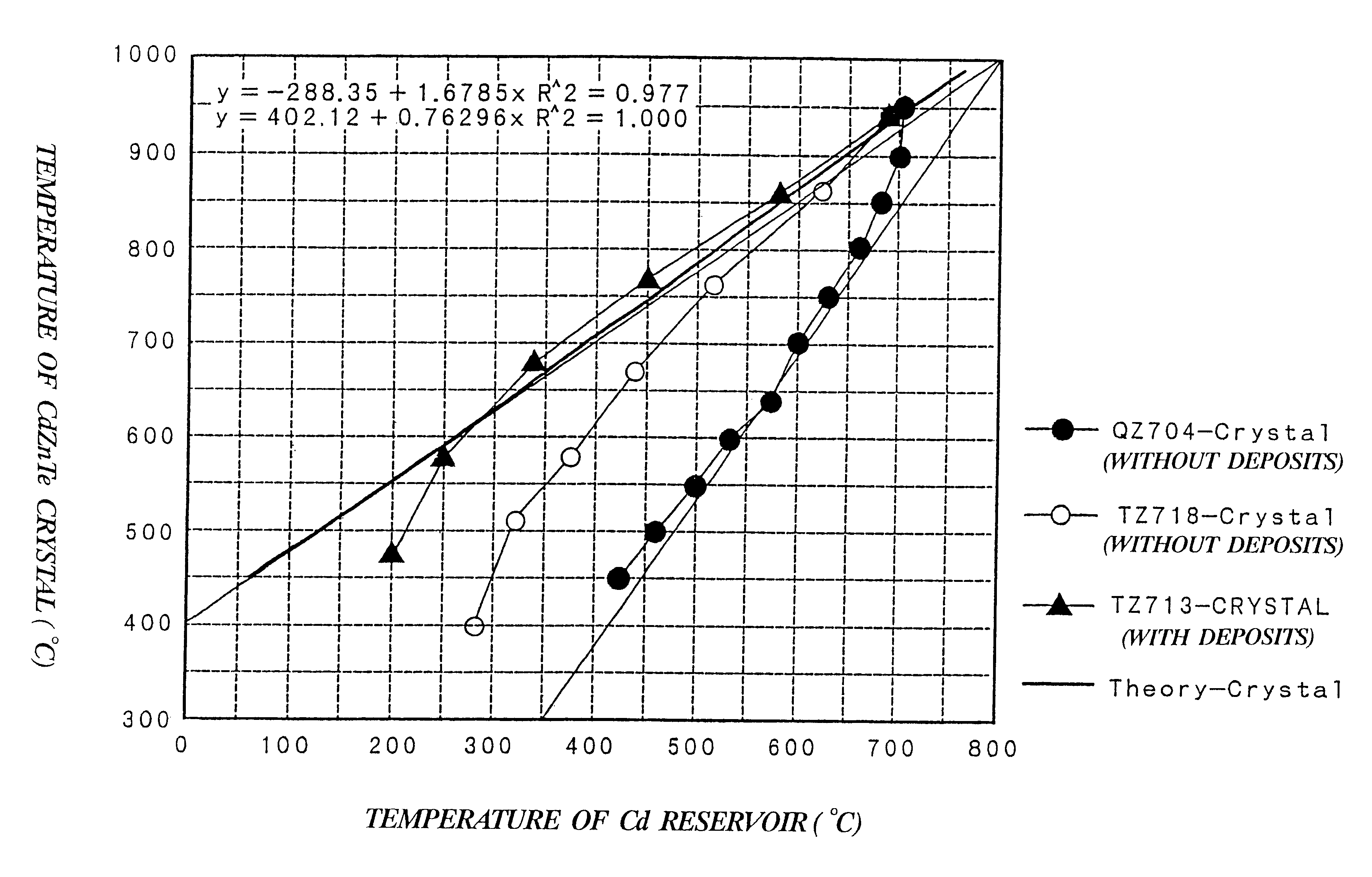
Hereinafter, as an example of the preferred embodiments of the present invention, the process for producing the CdZnTe crystal, to which the producing process according to the present invention is applied will be explained with reference to FIGS. 1 and 2.

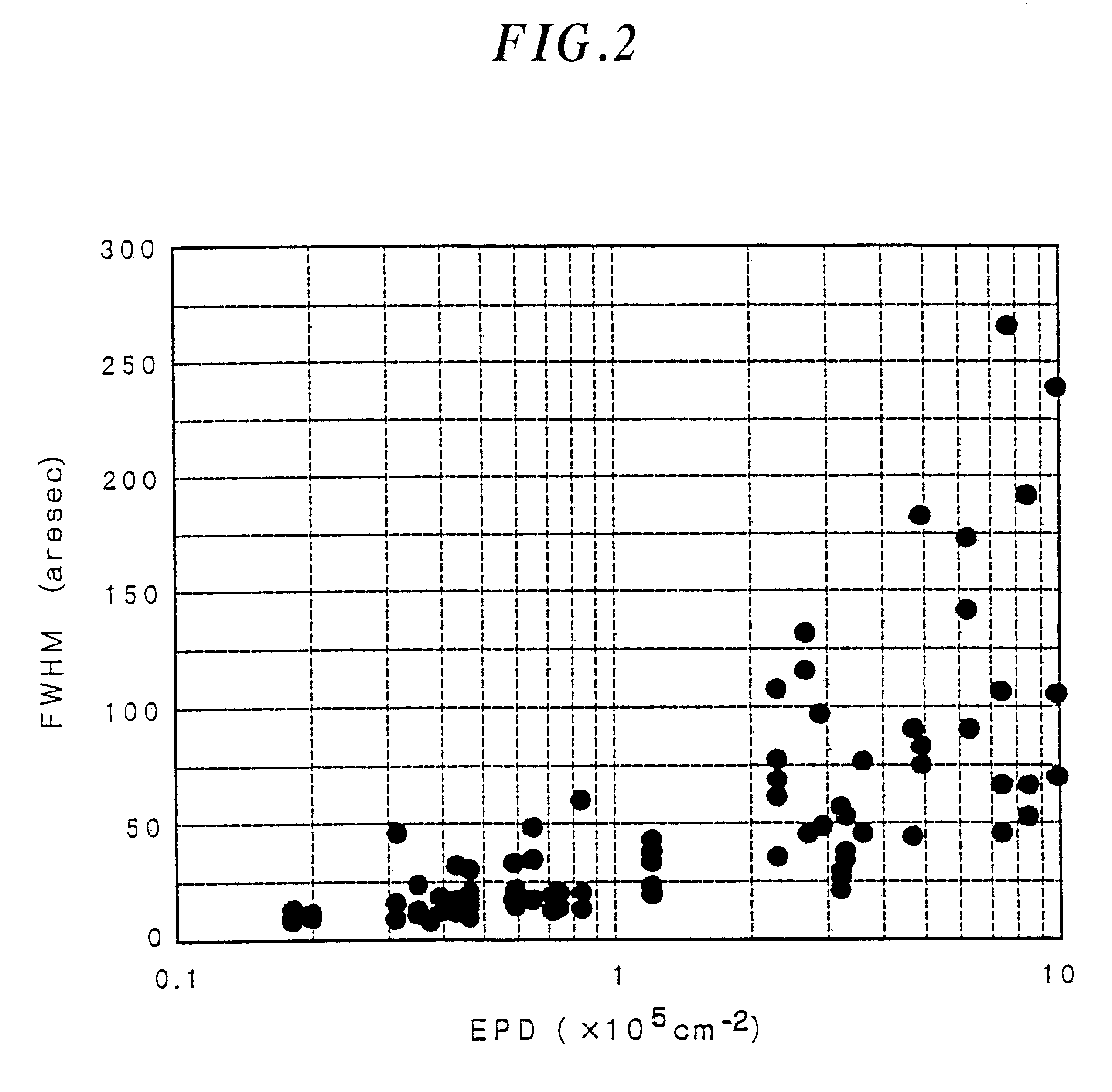
FIG. 1 is a graph showing the relationship between the temperature of the crystal and that of the Cd reservoir in the cooling step. FIG. 2 is a graph showing a correlation between the full-width-half-maximum (FWHM) of a double crystal X-ray rocking curve of the CdZnTe crystal and the etch pit density (EPD) thereof.

In the present embodiment, a CdZnTe crystal (Zn: 3.5%) having a size of 3".phi..times.6 cm and a mass of 1500 g was grown by the VGF method. After the crystal growing step was finished, the temperature of the crystal was decreased to 950.degree. C. From the result of the experience, it is confirmed that when the temperature of the crystal is from 700 to 1050.degree. C., the same effect can be obtained.

In order to keep the ...


PUM

PropertyMeasurementUnit
temperatureaaaaaaaaaa
particle diameteraaaaaaaaaa
pressureaaaaaaaaaa

Abstract

An object of the present invention is to reduce the etch pit density (EPD) and the full-width-half-maximum (FWHM) value of the double crystal X-ray rocking curve, and to provide a CdTe crystal or a CdZnTe crystal which does not include deposits having Cd or Te and the process for producing the same. After a CdTe crystal or a CdZnTe crystal was grown, while the temperature of the crystal is from 700 to 1050° C., the Cd pressure is adjusted so as to keep the stoichiometry of the crystal at the above temperature. The crystal is left for time t which is determined so that each of a diameter L(r) of the crystal and a length L(z) thereof satisfies the following equation 1:Then, when the crystal is cooled, the temperature of the crystal is decreased within a range in which the temperature of the crystal and that of a Cd reservoir satisfy the following equation 2:

Description

The present invention relates to a compound semiconductor single crystal and a process for producing the same. In particular, the present invention relates to an effective producing technique which is applied to a CdTe crystal or a CdZnTe crystal.BACKGROUND ON THE INVENTIONCompound semiconductor single crystals, such as cadmium telluride (CdTe), cadmium zinc telluride (CdZnTe) and the like, have advantages that a light emission efficiency thereof is higher than that of silicon (Si) and that a heterojunction can be applied thereto. The compound semiconductor single crystals are expected to be applied to a light emitting element, a photodetector, a low-noise amplifier, or the like.In particular, a CdTe crystal has a zinc blende structure, has a property that an energy gap thereof is 1.5 V and is a material which can have both a p-type conductivity and an n-type conductivity. Therefore, the CdTe crystal is used for semiconductor devices, such as a substrate for an epitaxial growth of a...

Claims


Application Information

Patent Timeline
Patent Type & Authority Patents(United States)
IPC IPC(8): C30B11/00
CPCC30B11/00C30B29/48
Inventor KOYAMA, AKIOHIRANO, RYUICHI
Owner JX NIPPON MINING & METALS CO LTD
Why Eureka
Try Eureka