Programmable logic datapath that may be used in a field programmable device

a logic and datapath technology, applied in the field of logic devices, can solve the problems of many instruction cycles, limited datapath of a cpu, and high speed requirements for relatively complex logic operations

Inactive Publication Date: 2002-02-26
PMC-SIERRA
View PDF29 Cites 94 Cited by
  • Summary
  • Abstract
  • Description
  • Claims
  • Application Information

AI Technical Summary

Problems solved by technology

Several aspects of a CPU's datapath may be limited by various device and / or design constraints.
In this way, a CPU may perform an arbitrarily complex logic operation, but it may take many instruction cycles to complete.
Some applications require relatively complex logic operations to be performed at high speed.
In many cases, this is not an economical way to implement demanding applications, while in others it is not possible at all.
However, PLAs, FPGAs and ASICs suffer from some limitations .
For example, ASICs cannot be reprogrammed.
Thus, such devices may not be suitable for applications wherein the execution of various logic operations may be required.
Furthermore, a substantial portion of circuitry in PLAs and FPGAs may be unused, resulting in power and / or cost inefficiency.
Although some FPGAs may be re-programmed to support various logic operations and numbers of inputs, such devices also suffer from limitations.
For example, in an SRAM cell-based FPGA, the interconnection array in which the various configurable logic blocks (CLBs) reside is typically programmed by pass transistors, which may result in relatively large "on" resistance.
Furthermore, interconnect delays in SRAM cell-based FPGAs may be relatively large due to certain wires of unpredictably varying, and sometimes relatively long, length.
Yet further inefficiency may be caused by the presence of multiple wires in the interconnect array which may be unused, resulting in increased capacitive load and increased device driver power requirements; and by the need for multiple pass transistors and SRAM cells to complete each logical connection.
Finally, the number of control / configuration bits typically required to program an FPGA (e.g., produce the appropriate interconnections between the CLBs) may exceed 250,000 bits, making dynamic (e.g., "on the fly"; on a cycle-by-cycle basis) reconfiguration / re-programming relatively difficult and commercially impractical.
However, the ASIC is not field programmable.
Finally, because the programmable logic datapath uses predefined connections, with selecting and routing performed by multiplexers, the speed of interconnection paths is increased while the unpredictability of this speed is greatly decreased.

Method used


Image

  • Programmable logic datapath that may be used in a field programmable device
  • Programmable logic datapath that may be used in a field programmable device
  • Programmable logic datapath that may be used in a field programmable device

Examples


Embodiment Construction

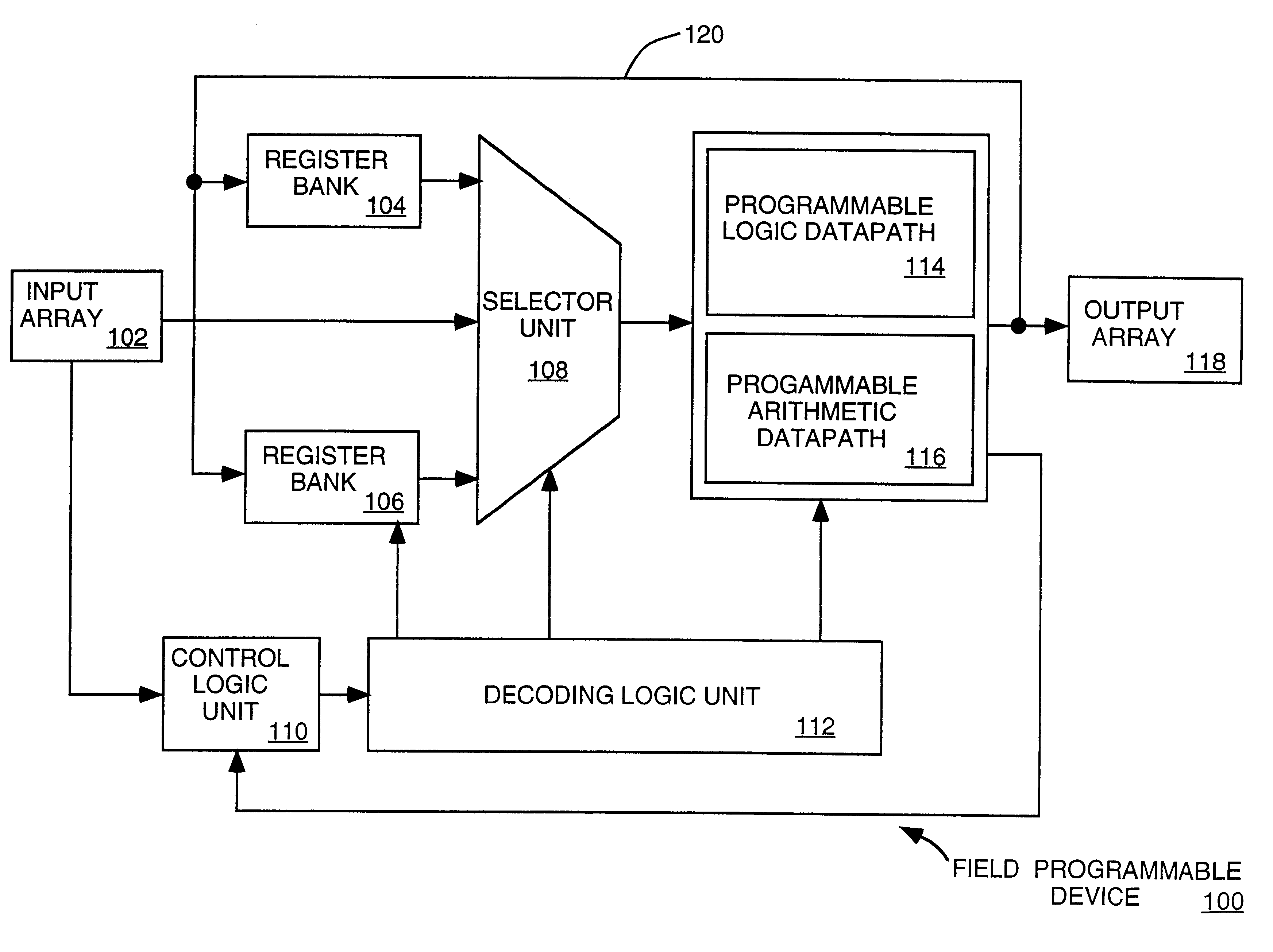
FIG. 1 is a block diagram illustrating a field programmable device according to one embodiment of the invention. In FIG. 1, a field programmable device 100 is shown which includes an input array 102 and an output array 118. The input array 102 represents one or more bits that are input to the field programmable device 100. Similarly, the output array 118 represents one or more bits that are output by the field programmable device 100. In one embodiment, the input array 102 and / or the output array 118 may represent registered / latched input and output bits, respectively.

The input array 102, a register bank 104, and a register bank 106 are shown coupled to a selector unit 108. The register banks 104 and 106 each represents a set of one or more registers / latches for storing data (or a subset thereof): 1) input into the input array 102; and / or 2) output by the datapath(s) provided via a feedback path 120. Thus, the register bank 104 and / or 106 may represent or include an accumulator, as ...


PUM


Abstract

A method and apparatus for providing a programmable logic datapath that may be used in a field programmable device. According to one aspect of the invention, a programmable logic datapath is provided that includes a plurality of logic elements to perform various (Boolean) logic operations. The programmable logic datapath further includes circuitry to selectively route and select operand bits between the plurality of logic elements (operand bits is used hereinafter to refer to input bits, logic operation result bits, etc., that may be generated within the logic datapath). In one embodiment, by providing control bits concurrently with operand bits to routing and selection (e.g., multiplexing) circuitry, the programmable logic datapath of the invention can provide dynamic programmability to perform a number of logic operations on inputs of various lengths on a cycle-by-cycle basis.

Description

1. Field of the InventionThe invention relates to the field of logic devices. More specifically, the invention relates to the field of programmable logic devices.2. Background InformationOne of the core functional units of a computer processor (or CPU) is the arithmetic / logic datapath, or simply, the datapath. The datapath is typically responsible for executing various arithmetic and / or logic operations supported by the instruction set architecture (ISA) of a computer system. As such, the datapath typically includes an arithmetic logic unit (ALU) that performs arithmetic / logic operations, an address generation unit to provide memory addresses, and a control unit to provide the proper control signals for the various devices of the datapath to perform the desired operation(s).The control signals that control the operations of the datapath may be considered as a vector of bits, which is known as a "direct control vector", since it directly controls the datapath operations. The width of...

Claims


Application Information

Patent Timeline
Patent Type & Authority Patents(United States)
IPC IPC(8): G06F9/302G06F9/305G06F9/38
CPCG06F9/3001G06F7/575G06F9/3897G06F9/30029
Inventor ABBOTT, CURTIS
Owner PMC-SIERRA
Why Eureka
Try Eureka