Method for modular laser diode assembly

a laser diode and modular technology, applied in the direction of semiconductor laser structure details, semiconductor laser arrangements, semiconductor lasers, etc., can solve the problems of limiting the development of economical products and devices incorporating laser diode arrays, diode bars not having optimal contact with the "heat sink" lower layer, and the method and configuration of disclosures are not conducive to diode bar alignmen

Inactive Publication Date: 2002-03-05
LASERTEL
View PDF35 Cites 72 Cited by
  • Summary
  • Abstract
  • Description
  • Claims
  • Application Information

AI Technical Summary

Problems solved by technology

The mounting of numerous bars into a single array historically has been a somewhat labor and / or cost intensive proposition, thus partially impeding the development of economical products and devices incorporating laser diode arrays.
However, the methods and configurations of the disclosures are not conducive to diode bar alignment, as the bars tend to tip and roll within the grooves during assembly.
The diode bars do not have optimal contact with the "heat sink" lower layer, and maximized alignment of the bars in the grooves also is not taught.
The disclosure teaches diversity in diode bar packing, and a configuration which possibly eases the replacement of defective individual bars, but is comparatively complex and expensive.
Diode bar alignment is not carefully optimized.

Method used


Image

  • Method for modular laser diode assembly
  • Method for modular laser diode assembly
  • Method for modular laser diode assembly

Examples


Embodiment Construction

)

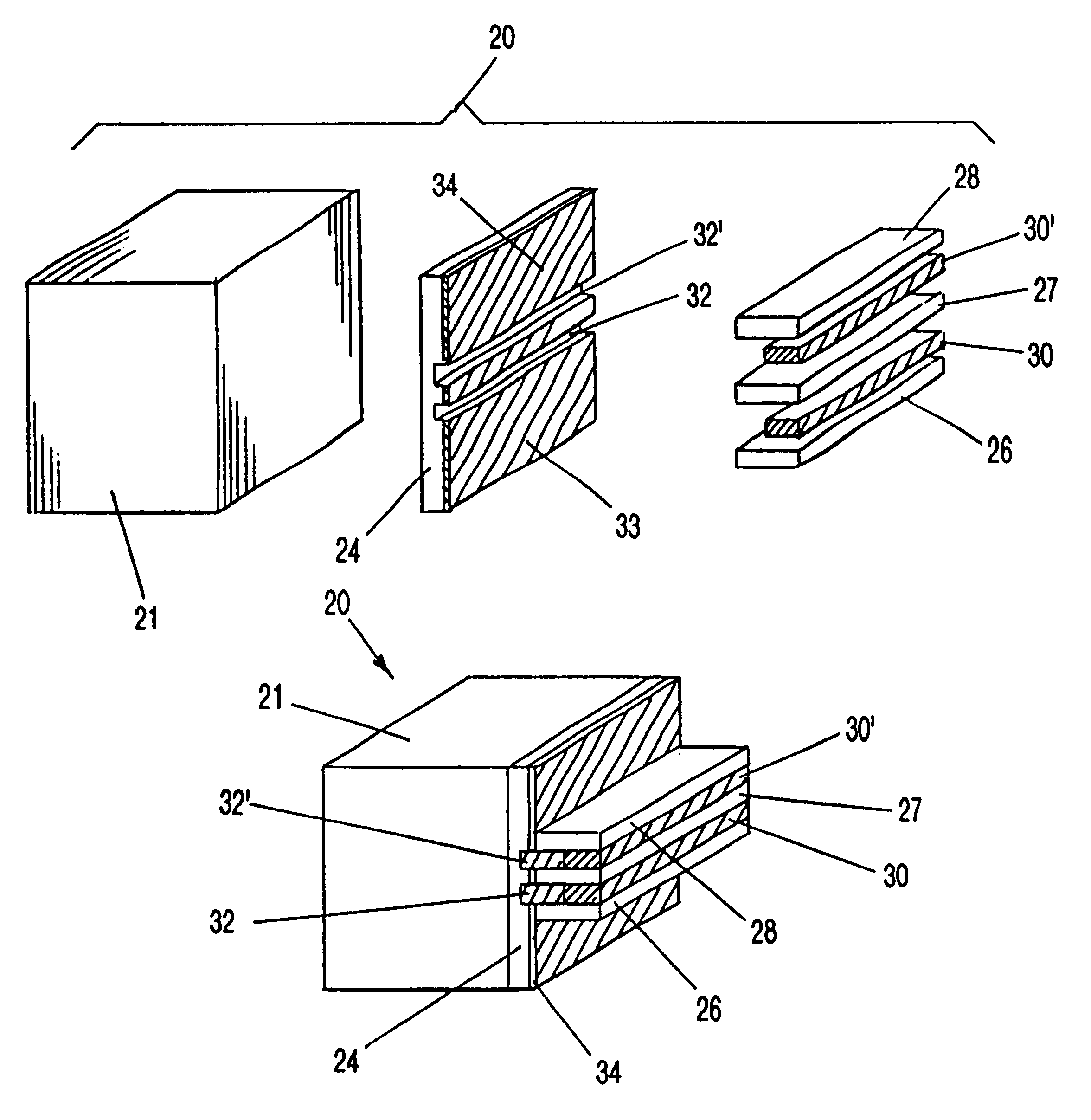
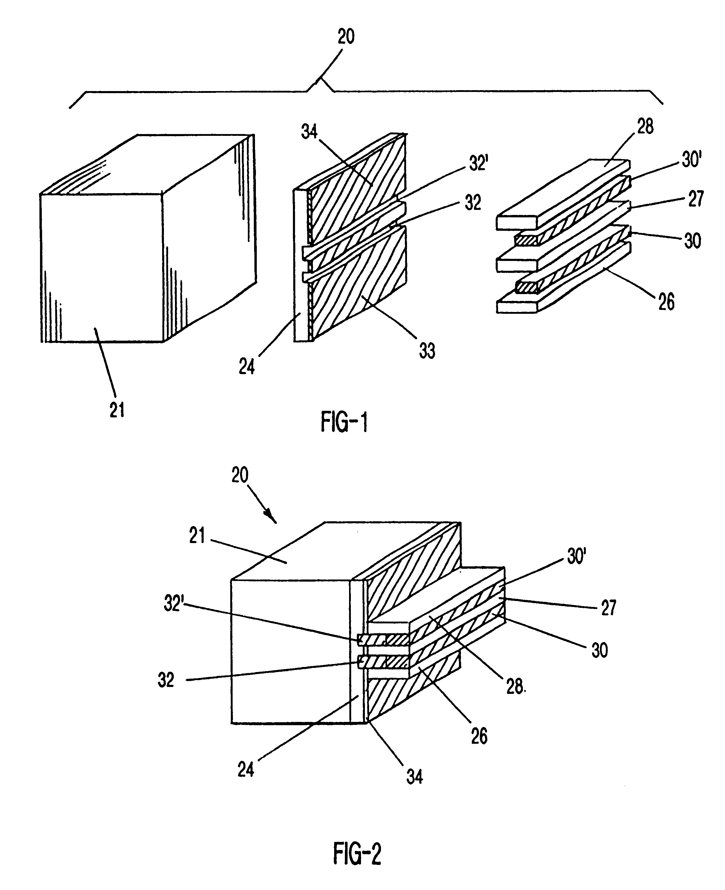
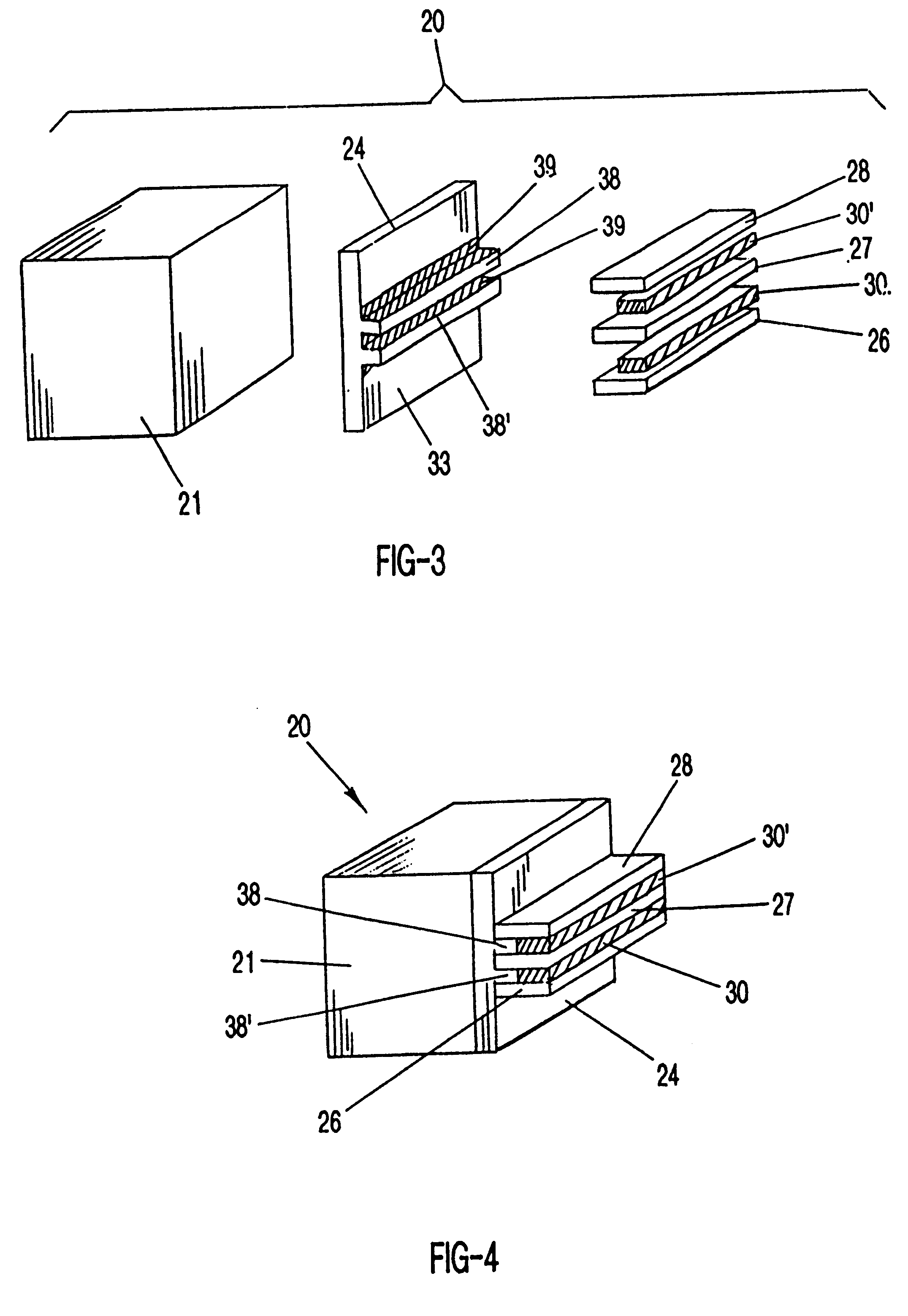
The present invention relates to laser diode apparatus and methods of assembly. The apparatus of the invention is an assembly of laser diode bars. By the apparatus and method of the invention, a laser diode bar assembly is provided having diode bars that are optimally aligned and may be densely packed. Parallelism of the diode bars is enhanced and diode bar curvature is eliminated. The apparatus of the invention manifests increased efficiencies in cooling and electrical continuity, and finds ready application in any area in which high power semiconductor laser arrays are used or desired. In one embodiment of the method of the invention, the array is composed of a plurality of separately constructed sub-modules, which permits individual diode bars to be pre-tested for performance or characteristics before installation on a substrate to define an array, or for individual post-installation replacement as needed.

The apparatus of the invention features two principal embodiments, a "stac...


PUM


Abstract

A method for laser diode bar assembly. A method for assembling a modular stacked diode array is disclosed, whereby a diode bar is bonded between a pair of conductive spacers, as by soldering, to create a diode submodule. Each submodule, prior to being affixed to a substrate, may be individually pre-tested. Any number of diode bar submodules then may be affixed to a substrate to construct a diode bar array. A stacked array embodiment assembled according to the method provides for efficient cooling of the diode bars and electrical connection between diode bars while maximizing alignment of the diode bars. The spacers are connected to a conductive surface on a heat spreader. In the stacked array, one or more diode bars are alternated in series with two or more conductive spacers, with a series circuit provided from diode bar to diode bar. The spacers hold the diodes spaced apart from insulating grooves in the conductive layer on the substrate. Alternatively, thermally conductive separator fins extend from the heat spreader substrate to contact the diode bars situated between the spacers to promote rapid heat transfer from the diodes while maintaining the diode bars electrically isolated from tie conductive layer on the substrate.

Description

1. Field of the Invention (Technical Field)The present invention relates to laser diodes, particularly to a laser diode assembly which promotes accurate spacing and alignment of diode bars, cooling of diode bars and electrical conductivity through the diode bars, as well as modularized assembly and pre-testing.2. Background ArtLaser diode arrays are in general use in a wide variety of industrial and research applications. Pluralities of diode bars are mounted up on a substrate to provide the multiplied power of numerous bars, versus the effect offered by a single bar. To optimize the efficiency of a multiple diode bar array, it is desirable not only that the diode bars be properly aligned so that their emitter surfaces face the same direction, but electrical conductivity between bars and cooling of the bars should be optimized.Most efforts in the art have focused upon modes and means of mounting numerous diode bars quickly and inexpensively. The mounting of numerous bars into a sing...

Claims


Application Information

Patent Timeline
Patent Type & Authority Patents(United States)
IPC IPC(8): H01S5/40H01S5/00H01S5/02
CPCH01S5/02264H01S5/02272H01S5/4043H01S5/4018H01S5/02476H01S5/02365H01S5/0237
Inventor HODEN, BRIAN P.
Owner LASERTEL
Why Eureka
Try Eureka