
Clock control circuit and clock control method

a clock control and clock technology, applied in the direction of generating/distributing signals, pulse techniques, oscillation generators, etc., to achieve the effect of uniform phase difference and greatly reduced jitter per frequency-multiplied clock

Inactive Publication Date: 2002-04-30
RENESAS ELECTRONICS CORP
View PDF3 Cites 93 Cited by
  • Summary
  • Abstract
  • Description
  • Claims
  • Application Information

AI Technical Summary

Benefits of technology

Accordingly, an object of the present invention, in one aspect, is to provide a clock control circuit and method as well as a semiconductor integrated circuit device in which center-frequency fluctuation caused when a PLL is used and jitter due to a feedback loop are eliminated to thereby reduce phase error to a major degree.
reducing jitter of a frequency-multiplied clock by generating multiphase clocks which are obtained by frequency multiplying an input clock, using a frequency multiplying interpolator which includes a plurality of circuits each of which is for outputting a signal obtained by internally dividing a phase difference between two signals;

Problems solved by technology

The clock control circuits according to the prior art described above have a number of problems described below.

Method used


Image

  • Clock control circuit and clock control method
  • Clock control circuit and clock control method
  • Clock control circuit and clock control method

Examples


second embodiment

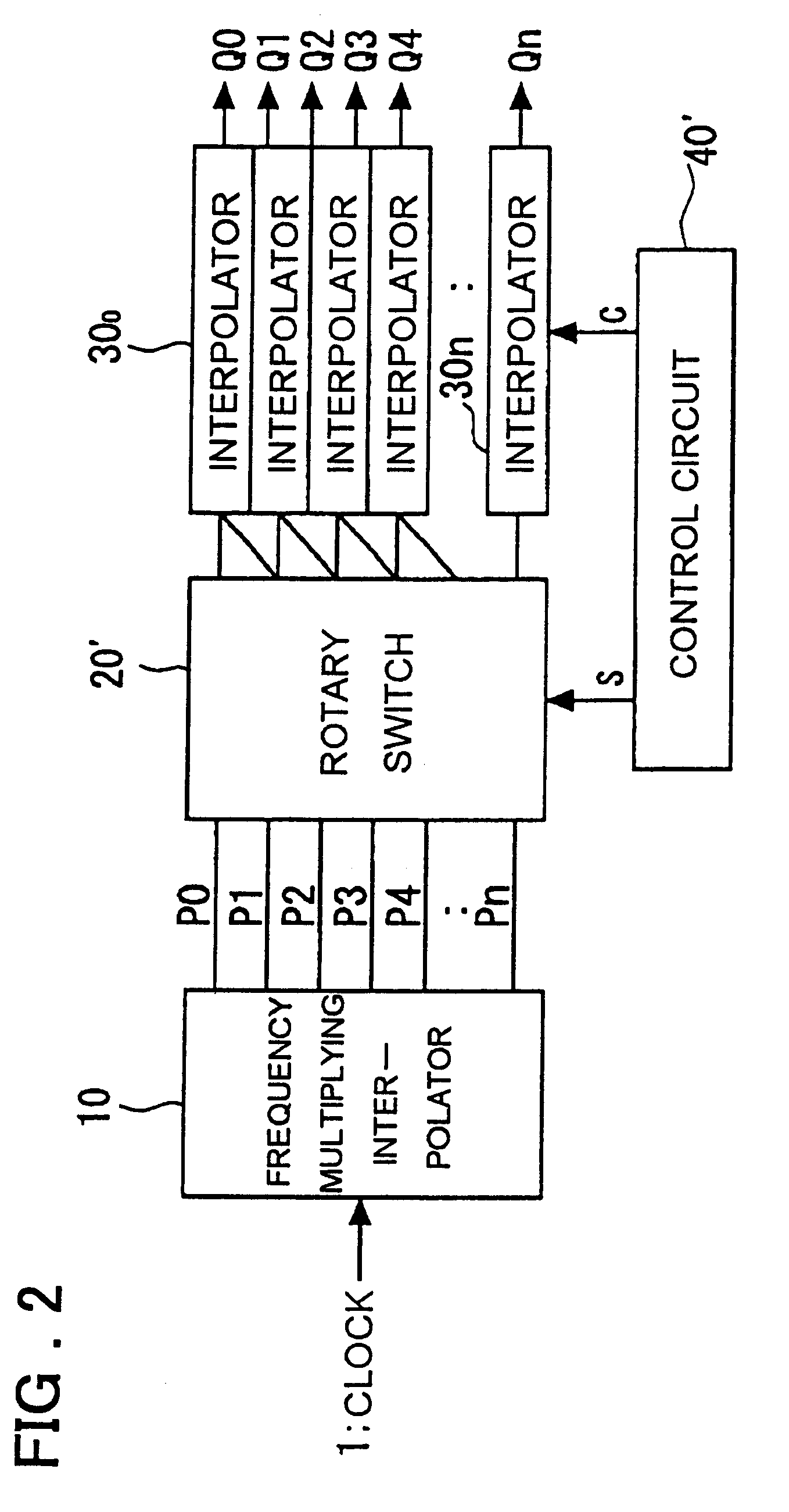
FIG. 2 is a block diagram illustrating the structure of the present invention.

As shown in FIG. 2, this embodiment differs from the first embodiment in that there are provided a plurality of interpolators 300 to 301 each of which outputs a signal obtained by internally dividing a phase difference between two signals output from a switch 20', the outputs of the interpolators constituting frequency-multiplied clocks Q0 to Qn. In the second embodiment, the structures of the frequency multiplying interpolator 10 and of the individual interpolators 300 to 301 are identical with those of the frequency multiplying interpolator 10 and interpolator 30 described in connection with the first embodiment.

FIG. 3 is a block diagram showing an example of the structure of the switch 20' and of the arrangement of the plurality of interpolators 30 according to the second embodiment of the invention.

As shown in FIG. 3, the switch 20' has a selector switch 20'-1 to which odd-phase clocks among the multip...

first embodiment

In a manner similar to that of the control circuit 40 described in conjunction with the first embodiment, the control circuit 40' comprises a counter and a decoder circuit and outputs the control signal C to each interpolator 30. If it is necessary to advance or delay phase further in a case where the internal-division ratio of an interpolator 30 has attained an upper or lower limit, the control circuit 40' exercises control to change over the odd-phase clock, which is supplied to the interpolator 30 as the first input signal, to the immediately adjacent odd-phase clock on either side, and to change over the even-phase clock, which is supplied to the interpolator 30 as the second input signal, to the immediately adjacent even-phase clock on either side.

FIG. 14 is a diagram showing results obtained by investigating the operation of a clock control circuit according to an embodiment of the present invention. FIG. 14 depicts the results obtained by using a circuit simulator (SPICE 2) t...

third embodiment

a clock control circuit according to the present invention will now be described with reference to the drawings.

FIG. 15 is a block diagram illustrating the structure of a clock control circuit according to a third embodiment of the present invention.

As shown in FIG. 15, the clock control circuit of the third embodiment uses shift-register-type counters 170, 171 and has phase adjusting interpolators 130, 131 serving as the control cirrcuit 40 of the first embodiment. The interolator 130 is for finely adjusting the phase difference between input clocks to 0.degree., and the fine adjusting interpolator 131 outputs a clock signal obtained by shifting phase by an amount equivalent to any angle (offset).

More specifically, as shown in FIG. 15, a multiphase frequency multiplying circuit 110 to which the input clock 1 is input for generating multiphase frequency-divided clocks is constituted by, e.g., the frequency multiplying interpolator 10 described in the foregoing embodiments. The multi...


PUM


Abstract

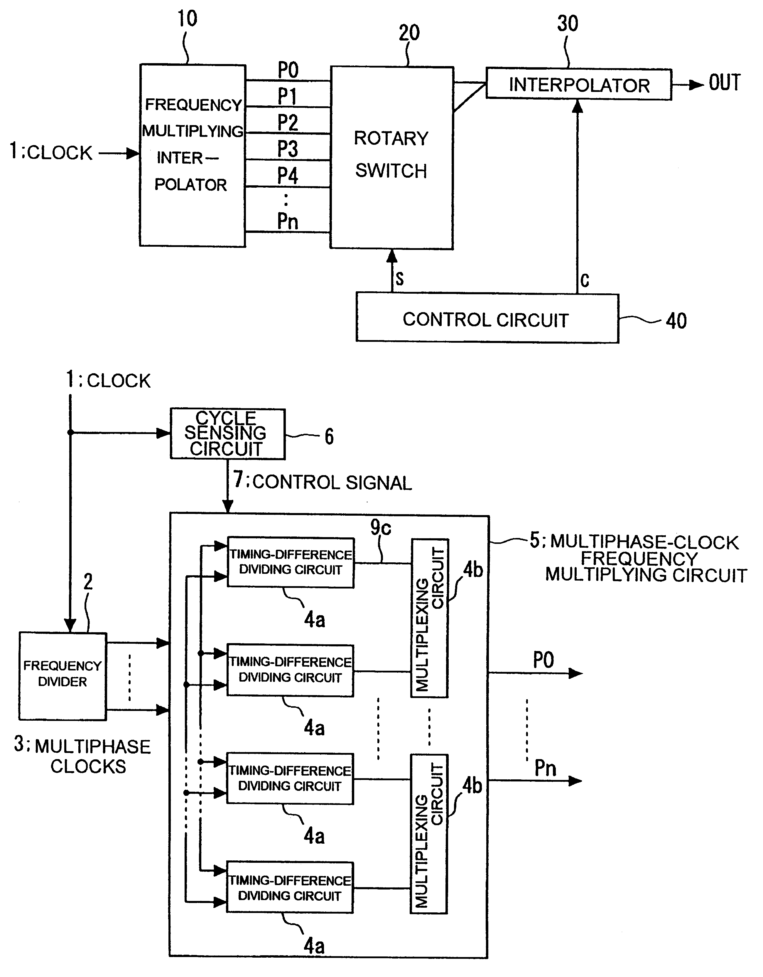
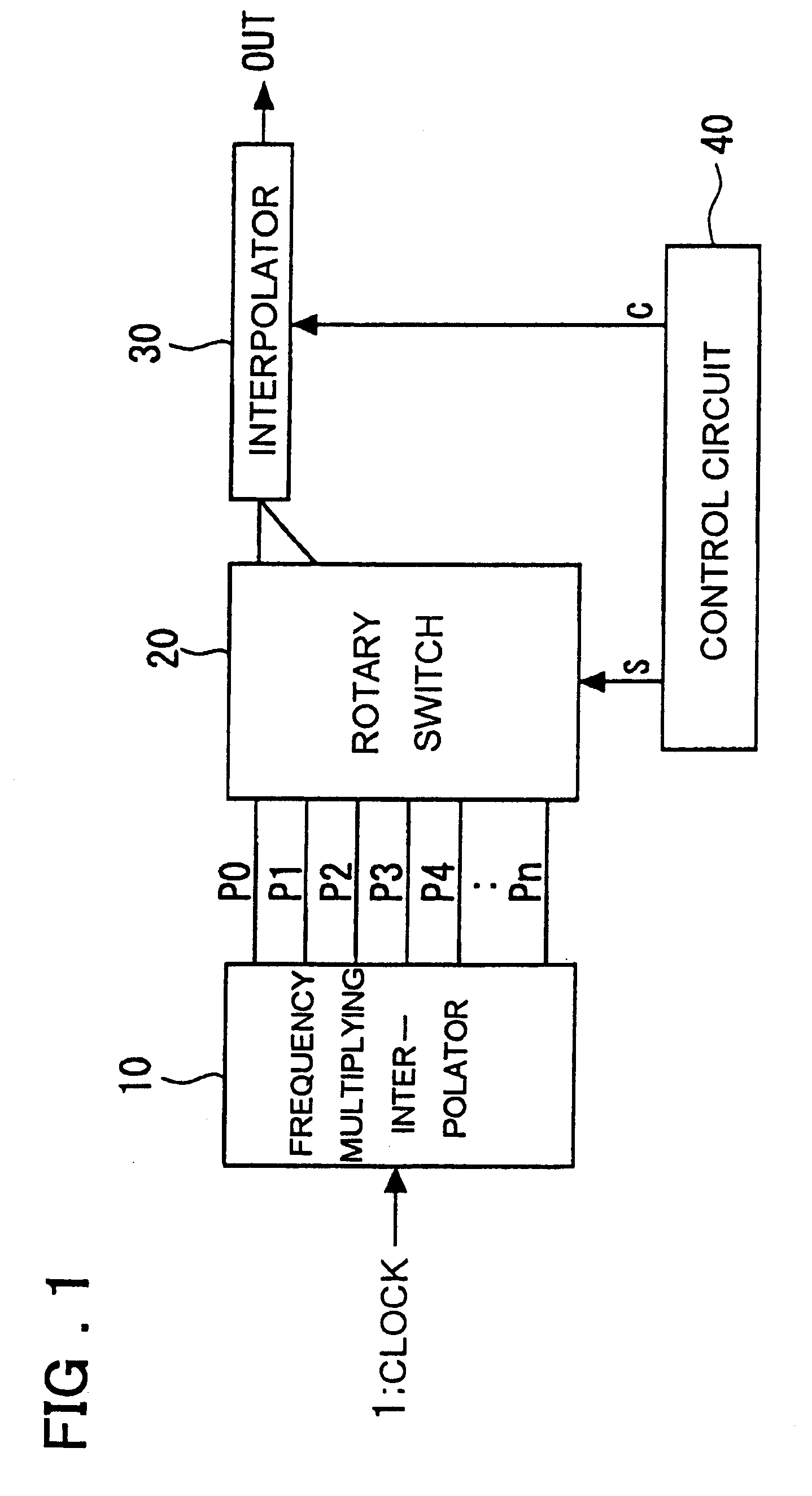
A clock control circuit which includes a frequency multiplying interpolator for generating and outputting multiphase clocks by frequency multiplying an input clock; a switch for outputting two of the multiphase clocks input thereto from the frequency multiplying interpolator; a fine adjusting interpolator, to which the two outputs from the switch are applied, for outputting a signal obtained by internally dividing the phase difference between the two outputs; and a control circuit for controlling the switching of the switch and varying the internal-division ratio of the fine adjusting interpolator.

Description

This invention relates to clock control technology and, more particularly, to a clock control circuit and method using an interpolator for frequency multiplication.In order to deal with an increase in the scale of circuitry that can be integrated on a single chip and in order to handle higher operating frequencies, semiconductor integrated circuits which include a synchronizing circuit that operates upon being supplied with a clock are provided with a clock control circuit for controlling phase and frequency of clocks externally and internally of the chip.A PLL (Phase-Locked Loop) or a DLL (Delay-Locked Loop) is used conventionally as such a clock control circuit. In semiconductor circuits having system-scale circuitry on a single chip such as an LSI chip (referred to also as a "system on silicon"), it is now necessary to provide a clock control circuit for phase and frequency control for each macroblock within the chip, by way of example.In addition to use of a PLL or DLL as the co...

Claims


Application Information

Patent Timeline
Patent Type & Authority Patents(United States)
IPC IPC(8): H03K5/00G06F1/06H03L7/00H03L7/081
CPCH03K5/131H03K5/135H03K5/156H03L7/0814H03L7/07H03L7/0805H03K2005/00052H03L7/0816H03L7/00
Inventor SAEKI, TAKANORI
Owner RENESAS ELECTRONICS CORP
Learn More