Apparatus and method for serial data communication between plurality of chips in a chip set

a technology of serial data communication and chip set, applied in the field of data communication, can solve the problems of increasing the size of the package in proportion to increasing the complexity of the assembly of the chip set, increasing the manufacturing cost, etc., and achieve the effect of reducing the number of signal lines

Inactive Publication Date: 2002-04-30
UNITED MICROELECTRONICS CORP
View PDF2 Cites 72 Cited by
  • Summary
  • Abstract
  • Description
  • Claims
  • Application Information

AI Technical Summary

Benefits of technology

to provide an apparatus for serial data communication using a reduced number of signal lines among a plurality of IC chips.
In accordance with the foregoing and other objects of the invention, a new and improved apparatus for serial data communication among a plurality of IC chips is provided. In the apparatus, one IC chip acts as a master, while the other chip(s) are slaved to the master. In response to conditions internal to the master chip, or in response to a request from at least one slave chip, the master chip generates a transfer control signal and a synchronization clock signal. The transfer control signal defines a transfer phase during which data transfer among the chips can take place. The chips take turns sending and receiving data in a multiplexed fashion, with sending and receiving parties designated by a count of synchronization clock signal cycles. The synchronization clock signal is generated at a high frequency, to allow fast data transfer. The data communication between the IC chips requires only a reduced number of signal lines, which allows the number of pins required for connection of the two IC chips, as well as manufacturing costs, to be significantly reduced.
The data communication between the IC chips requires only a reduced number of signal lines, which allows the number of pins required for connection of the two IC chips, as well as manufacturing costs, to be significantly reduced.

Problems solved by technology

First, the size of the package increases in proportion to the number of signal lines.
Second, the complexity of assembly of the chip set increases as the number of signal lines increases.
Third, manufacturing cost is increased due to an increase in the chip area required to accommodate the large number of signal lines.
There are, however, two drawbacks to the system configuration of FIG. 1.
Second, power consumption in the chip set is very high.
There are, however., two drawbacks to the system configuration of FIG. 2.
Therefore, the system configuration of FIG. 2 is not suitable for data communication among a large number of IC chips.

Method used


Image

  • Apparatus and method for serial data communication between plurality of chips in a chip set
  • Apparatus and method for serial data communication between plurality of chips in a chip set
  • Apparatus and method for serial data communication between plurality of chips in a chip set

Examples


Embodiment Construction

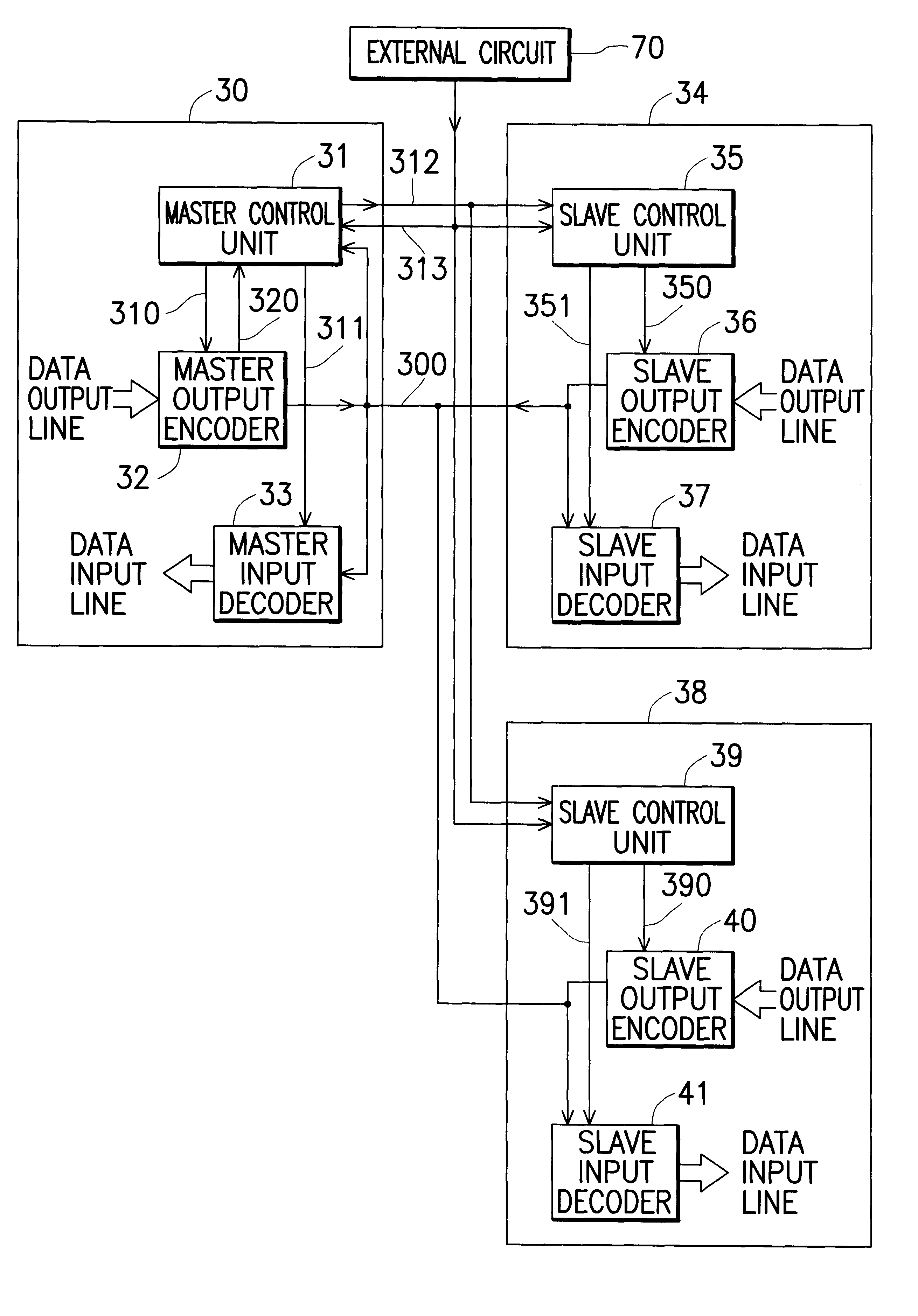
Referring to FIG. 3, there is shown a preferred embodiment of the apparatus according to the invention, which is used for data communication among three separate IC chips 30, 34, 38. It is to be understood that, broadly speaking, the invention can be used for data communication among a smaller or larger plural number of IC chips or among a plurality of source devices and a plurality of associated destination devices and that communication among three IC chips is described by way of example only.

According to the invention, one chip is designated a master chip and the remainder of the chips are slaved to it. In FIG. 3, the first IC chip 30 is designated the master, and the IC chips 34 and 38 are the slaves.

The first IC chip 30 includes a master control unit 31, a master output encoder 32, and a master input decoder 33; the second IC chip 34 includes a slave control unit 35, a slave output encoder 36, and a slave input decoder 37; and the third IC chip 38 includes a slave control unit ...


PUM


Abstract

An apparatus for serial data communication between a plurality of IC chips with a reduced number of inter-chip signal lines. In the apparatus, one IC chip acts as a master, while the other chip(s) are slaved to it. In response to conditions internal to the master chip or in response to a request from at least one of the slave chips, the master chip generates a transfer control signal and a synchronization clock signal. The transfer control signal defines a transfer phase during which data transfer among the chips can take place. The chips take turns sending and receiving data in a multiplexed fashion. with sending and receiving parties designated by a count of synchronization clock signal cycles. The synchronization clock signal is generated at a high frequency, to allow fast data transfer.

Description

1. Field of the InventionThe invention relates to data communication, and more particularly, to an apparatus for serial data communication among a plurality of integrated circuit ("IC") chips which allows a reduced number of signal lines to be interconnected among the IC chips.2. Description of the Related ArtIn a chip set that includes several IC chips, a number of signal lines are often interconnected among the IC chips for data transmission among the same. The provision of a large number of signal lines in a chip set has several drawbacks. First, the size of the package increases in proportion to the number of signal lines. Second, the complexity of assembly of the chip set increases as the number of signal lines increases. Third, manufacturing cost is increased due to an increase in the chip area required to accommodate the large number of signal lines.It is a customary practice to arrange the signal lines in parallel between two separate IC chips in order to attain a high data ...

Claims


Application Information

Patent Timeline
Patent Type & Authority Patents(United States)
IPC IPC(8): H04L23/00H04L7/00
CPCG06F13/4282
Inventor LEE, DAVIDHUANG, CHENG-WANG
Owner UNITED MICROELECTRONICS CORP
Why Eureka
Try Eureka